Plasmon waveguide and optical element using the same

a technology of optical elements and waveguides, applied in the direction of optical waveguide light guides, instruments, nanotechnology, etc., can solve the problems of large loss, communication difficulty, and the dimension of waveguides cannot be reduced to equal or less than the wavelength used, and achieves simple structure, increased transmittance, and high wavelength selectivity

Inactive Publication Date: 2011-05-05
KEIO UNIV
View PDF12 Cites 14 Cited by
  • Summary
  • Abstract
  • Description
  • Claims
  • Application Information

AI Technical Summary

Benefits of technology

[0033]According to the present invention, there can be provided a plasmon waveguide having a short element length in the incident-light traveling direction and a simple structure, and having high wavelength selectivity. Further, it is possible to increase the transmittance with a bent waveguide. Further, it is possible to make the plasmon waveguide function as an optical demultiplexer or multiplexer having high wavelength selectivity.

Problems solved by technology

However, a transmission loss becomes large at high frequency, which makes communication difficult.
However, in a conventional optical waveguide including a dielectric core and a cladding, the dimension of the waveguide cannot be reduced to equal or less than the wavelength used.

Method used


Image

  • Plasmon waveguide and optical element using the same
  • Plasmon waveguide and optical element using the same
  • Plasmon waveguide and optical element using the same

Examples


first embodiment

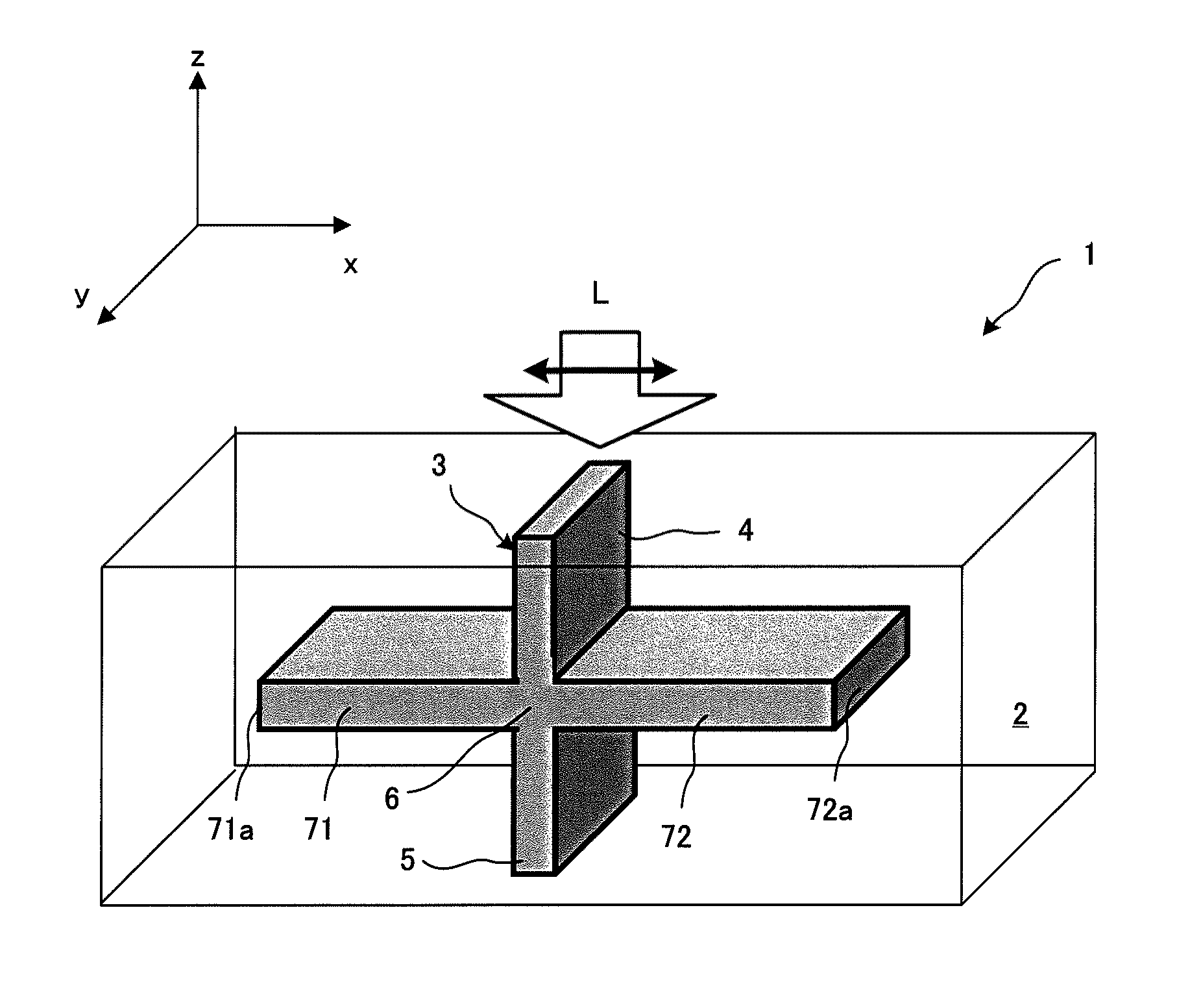
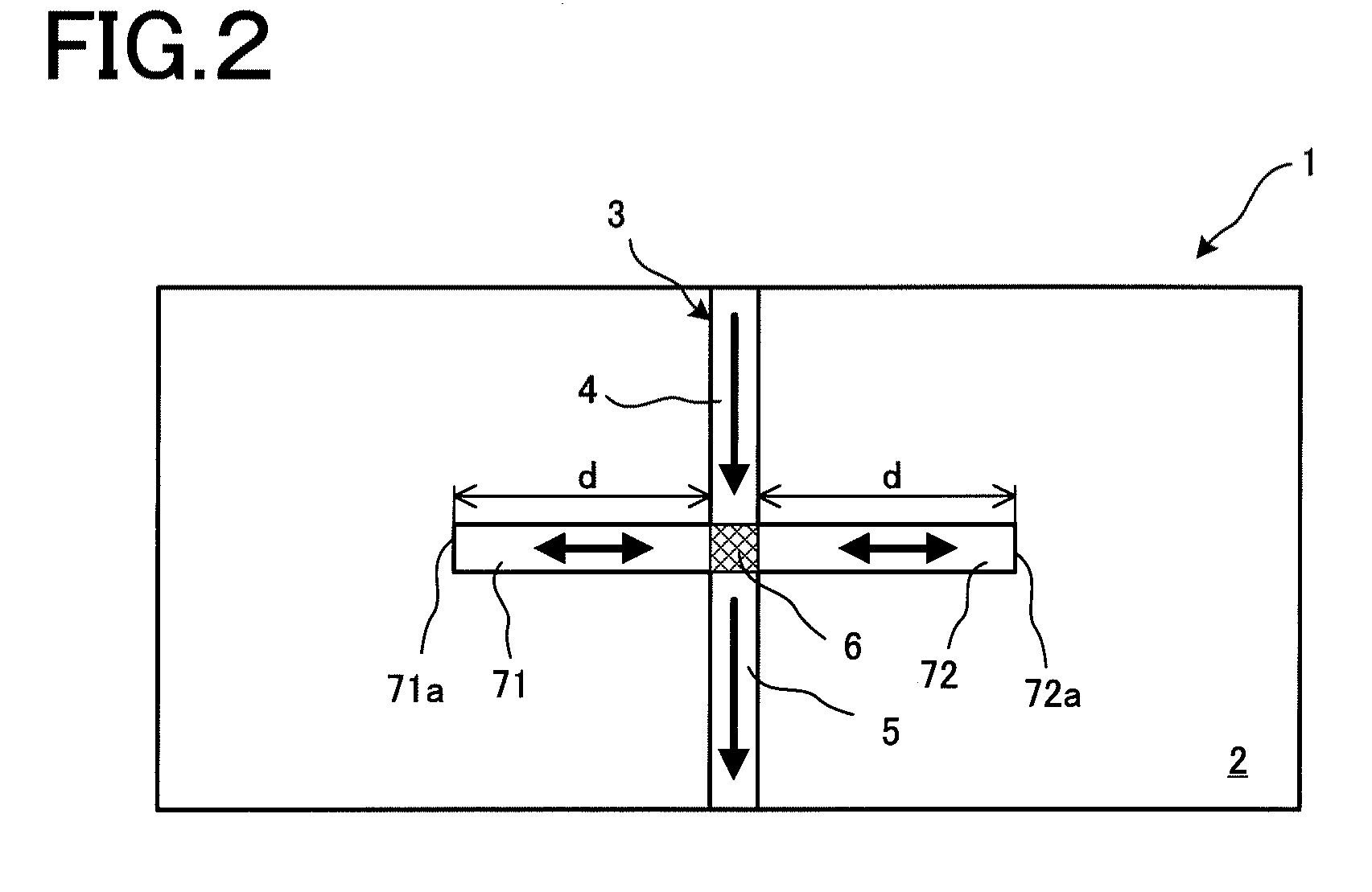
[0061]The incident-side plasmon waveguide 4 is disposed on the incident side of the light L with respect to the connection portion 6, to which polarized light L is incident. The emission-side plasmon waveguide 5 is disposed on the emission side of the light L with respect to the connection portion 6, from which the light L is emitted. The connection portion 6 connects the incident-side plasmon waveguide 4 and emission-side plasmon waveguide 5. In the first embodiment, the light traveling direction in the incident-side plasmon waveguide 4 and that in the emission-side plasmon waveguide 5 are the same.

[0062]The plasmon interference structure 7 extends from the connection portion 6 in the direction intersecting the incident-side plasmon waveguide 4 or emission-side plasmon waveguide 5 and has a termination 7a at which the light L is reflected.

[0063]The plasmon interference structure 7 of the first embodiment includes a first plasmon interference structure 71 and a second plasmon interf...

second embodiment

[0085]The second embodiment aims to provide a bent plasmon waveguide having a simple structure and small loss.

[0086]FIG. 7 is a perspective view of a plasmon waveguide according to the second embodiment, and FIG. 8 is a cross-sectional view of the plasmon waveguide according to the second embodiment.

[0087]The plasmon waveguide 1 according to the second embodiment includes a cladding 2 made of metal and a dielectric core 3 and provided with an incident-side plasmon waveguide 4, an emission-side plasmon waveguide 5 extending in a different direction from the incident-side plasmon waveguide 4, a connection portion 6 connecting the incident-side plasmon waveguide 4 and the emission-side plasmon waveguide 5, and a first plasmon interference structure 71 and a second plasmon interference structure 72 protruding from the connection portion 6 in the direction intersecting the emission-side plasmon waveguide 4 and incident-side plasmon waveguide 4, respectively, wherein the first plasmon int...

third embodiment

[0112]The third embodiment aims to provide an optical wavelength multiplexer / demultiplexer that can be used in the plasmon waveguide.

[0113]FIG. 13 is a perspective view of the plasmon waveguide according to the third embodiment, and FIG. 14 is a cross-sectional view of the plasmon waveguide according to the third embodiment.

[0114]The plasmon waveguide 1 according to the third embodiment includes a cladding 2 made of metal and a dielectric core 3 and is provided with an incident-side plasmon waveguide 4, a first emission-side plasmon waveguide 51, a second emission-side plasmon waveguide 52, a first connection portion 61 connecting the incident-side plasmon waveguide 4 and first emission-side plasmon waveguide 51, a second connection portion 62 connecting the incident-side plasmon waveguide 4 and second emission-side plasmon waveguide 52, a first plasmon interference structure 71 protruding from the first connection portion 61 in the direction intersecting the incident-side plasmon w...


PUM


Abstract

Disclosed is a plasmon waveguide including cladding (2) consisted of metal, and a dielectric core (3) which is formed of a transparent material, surrounded by or sandwiched by the cladding (2), and has at least one cross-section having a thickness no more than the wavelength of the incident light. The plasmon waveguide is provided with: a incident-side plasmon waveguide (4) into which light (L) is incident; an emission-side plasmon waveguide (5) from which light (L) is emitted; a connection portion (6) connecting the incident-side plasmon waveguide (4) and emission-side plasmon waveguide (5); and a plasmon interference structure (7) which extends from the connection portion (6) in the direction intersecting the incident-side plasmon waveguide (4) or the emission-side plasmon waveguide (5), and has a terminal (7a) at which light (L) is reflected.

Description

TECHNICAL FIELD[0001]The present invention relates to a plasmon waveguide for use in an optical circuit and an optical element using the same.BACKGROUND ART[0002]Along with the advancement of highly-networked information society, an increase in the communication speed in an electronic circuit has been promoted. However, a transmission loss becomes large at high frequency, which makes communication difficult. Under such a circumstance, there is a strong demand for development of optical circuits capable of achieving high communication speed, and some of which have already been utilized.[0003]In recent years, in order to respond to a demand for higher integration in the optical circuit, optical integration has been studied. However, in a conventional optical waveguide including a dielectric core and a cladding, the dimension of the waveguide cannot be reduced to equal or less than the wavelength used. That is, there is a lower limit on the dimension of the waveguide.[0004]A surface pl...

Claims


Application Information

Patent Timeline
Patent Type & Authority Applications(United States)
IPC IPC(8): G02B6/26G02B6/02
CPCG02B6/1226B82Y20/00
Inventor OBARA, MINORUOMODANI, SATOSHI
Owner KEIO UNIV
Why Eureka
Try Eureka