

Graphene sheet, graphene base including the same, and method of preparing the graphene sheet
- Summary
- Abstract
- Description
- Claims
- Application Information
AI Technical Summary
Benefits of technology
Problems solved by technology
Method used
Image

Examples
example 1
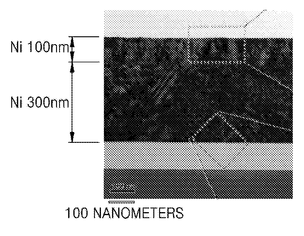
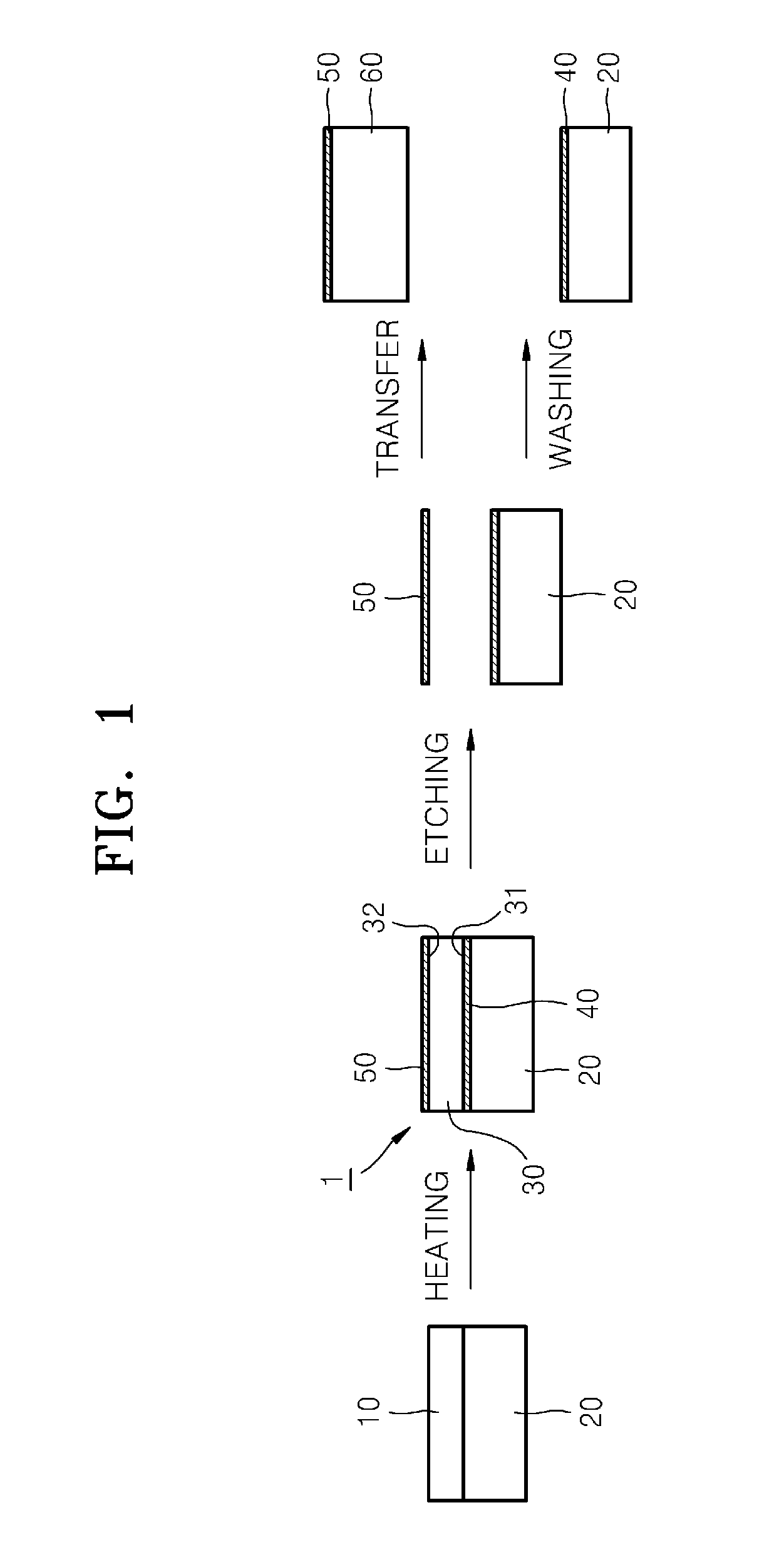
Nickel was deposited by e-beam evaporation on a 5 centimeter (cm) by 2 cm silicon substrate, which was coated with a 100 nm-thick SiO2 layer, to form a nickel (Ni) layer having a thickness of 300 nm on the silicon substrate.
The substrate with the Ni layer was immersed in 100 milliliters (mL) of triethylene glycol, maintained at 240° C. for 30 hours, and then cooled. The substrate was removed from the solution and ultrasonically washed with water, ethanol, and then acetone. The substrate was dried, placed in a reaction chamber under an argon atmosphere, heated at a rate of 100° C. per minute to 900° C., maintained at 900° C. for 30 seconds, and then cooled at a rate of 20° C. per minute to form a graphene sheet.
For analysis purposes, Ni was additionally deposited on the substrate with the graphene sheets to a thickness of about 100 nm and then milled. A cross-section of the resulting structure was analyzed by transmission electron microscopy (“TEM”). The results of the TEM analysis a...
example 2
Nickel was deposited by e-beam evaporation on a 5 cm by 2 cm silicon substrate, which was coated with a 100 nm-thick SiO2 layer 920, to form an Ni layer having a thickness of 200 nm on the silicon substrate. The Ni layer was patterned to provide a predetermined shape by photolithography to have a width of 200 μm in a center region thereof and a width of 30 μm in edge regions thereof.
The substrate with the patterned Ni layer was immersed in 100 mL of triethylene glycol, maintained at 240° C. for 30 hours and then cooled. The substrate was removed from the solution and ultrasonically washed with water, ethanol, and then acetone. The substrate was dried, placed in a reaction chamber under an argon atmosphere, heated at a rate of 100° C. per minute to 900° C., maintained at 900° C. for 30 seconds, and then cooled at a rate of 20° C. per minute to form patterned graphite sheets.
The substrate with the graphene sheets was immersed in a Ni etchant solution (TFB, available from TRANSENE COMP...
example 3
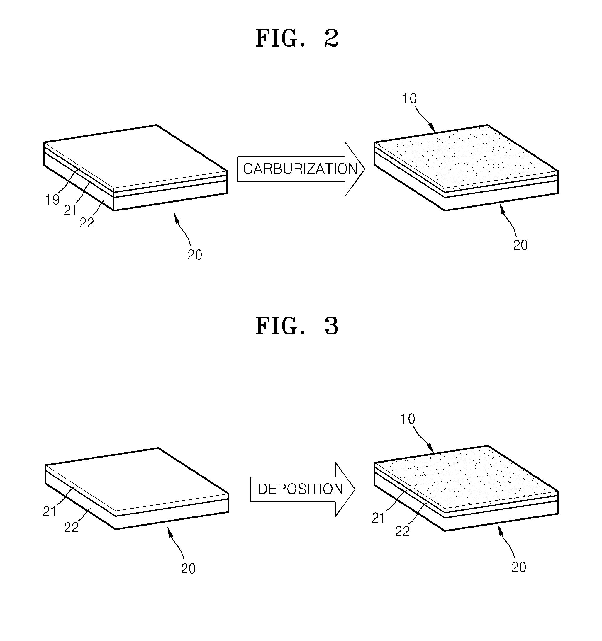
Separate Ni and Cu targets and a mixed gas of acetylene and Ar (1% by volume acetylene in Ar) were sputtered at a power of 700 watts (W) onto a 4″ diameter silicon substrate, which was coated with a 100 nm-thick SiO2 layer, then heated in a H2 atmosphere at 500° C. for 10 minutes, and then heated in an Ar atmosphere at 1000° C. for 30 seconds to provide the substrate with graphene sheets.
The substrate with the graphene sheets was immersed in a 0.01 M aqueous solution of FeCl3 to remove the Ni / Cu metal layer, removed from the aqueous solution, and then washed with water to recover the graphene sheet grown directly on the substrate. An optical micrograph and a Raman spectrum of the recovered graphene sheet, which had been grown between the substrate and the Ni layer, were obtained. The results are shown in FIGS. 10A and 10B.
FIG. 10A is an optical micrograph of a 0.01 mm2 area of the graphene sheet. FIG. 10A shows that the imaged area is completely filled with graphene, and devoid of a...
PUM
| Property | Measurement | Unit |
|---|---|---|
| Temperature | aaaaa | aaaaa |
| Fraction | aaaaa | aaaaa |
| Time | aaaaa | aaaaa |
Abstract
Description
Claims
Application Information