

Isolation structures for soi devices with ultrathin soi and ultrathin box
a soi and box technology, applied in the field of soi-based semiconductor devices, can solve the problems of leakage current and leakage current in the soi-based semiconductor devices
- Summary
- Abstract
- Description
- Claims
- Application Information
AI Technical Summary
Benefits of technology
Problems solved by technology
Method used
Image

Examples
first embodiment
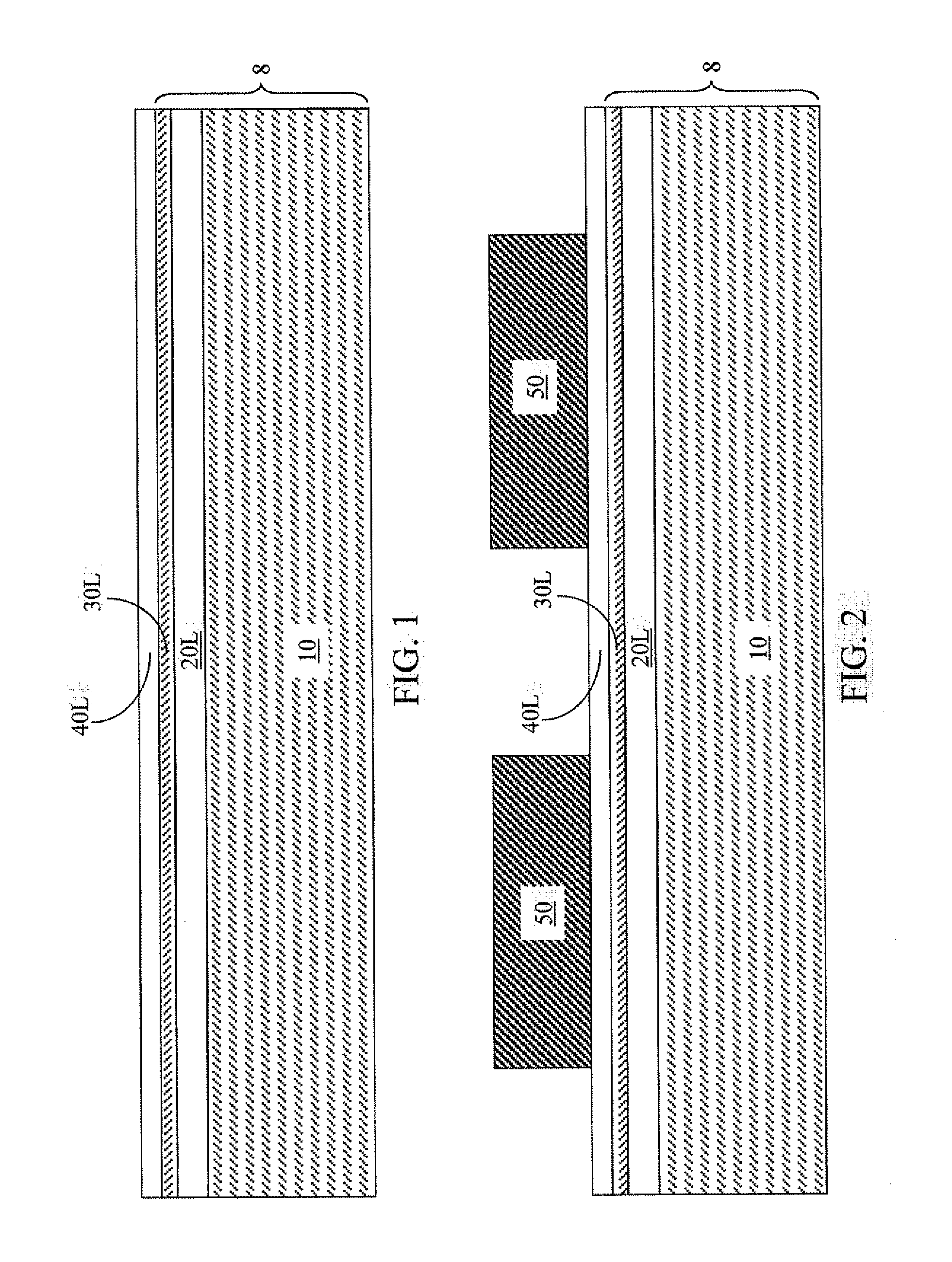
[0028]Referring to FIG. 1, a first exemplary semiconductor structure according to the present invention includes a substrate 8 and a dielectric oxide layer 40L formed on a top surface thereof. The substrate 8 can be a semiconductor-on-insulator (SOI) substrate that includes a vertical stack, from bottom to top, of a handle substrate 10, a buried insulator layer 20L located above the handle substrate 10, and semiconductor material layer 30L, located on an upper surface of the buried insulator layer 20L.
[0029]The handle substrate 10 includes a first semiconductor material, which can be selected from, but is not limited to, silicon, germanium, silicon-germanium alloy, silicon carbon alloy, silicon-germanium-carbon alloy, gallium arsenide, indium arsenide, indium phosphide, III-V compound semiconductor materials, II-VI compound semiconductor materials, organic semiconductor materials, and other compound semiconductor materials. Further, the material of the handle substrate 10 can be a s...
second embodiment
[0050]Referring to FIG. 11, a second exemplary semiconductor structure according to the present invention includes a substrate 8 and a dielectric oxide layer 40L formed on a top surface thereof. The substrate 8 can be a semiconductor-on-insulator (SOI) substrate that includes a vertical stack, from bottom to top, of a handle substrate 10, a buried etch-resistant dielectric layer 12L, a buried insulator layer 20L located above the buried etch-resistant dielectric layer 12L, and semiconductor material layer 30L located on an upper surface of the buried insulator layer 20L. Each of the handle substrate 10, the buried insulator layer 20L, and the semiconductor material layer 30L can have the same thickness, the same compositional characteristics, and the same structural characteristics as in the first exemplary semiconductor structure except that the buried etch-resistant dielectric layer 12L is located between the handle substrate 10 and the buried insulator layer 20L. The dielectric o...
third embodiment
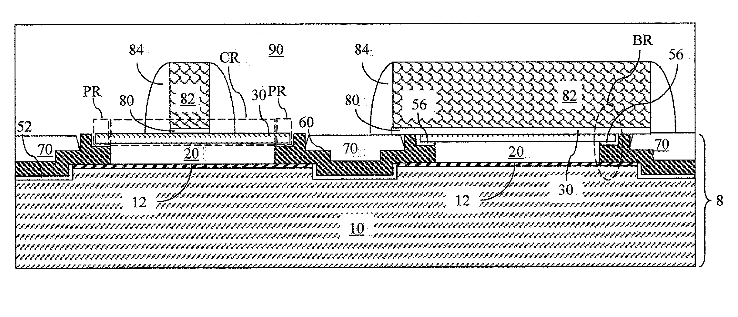
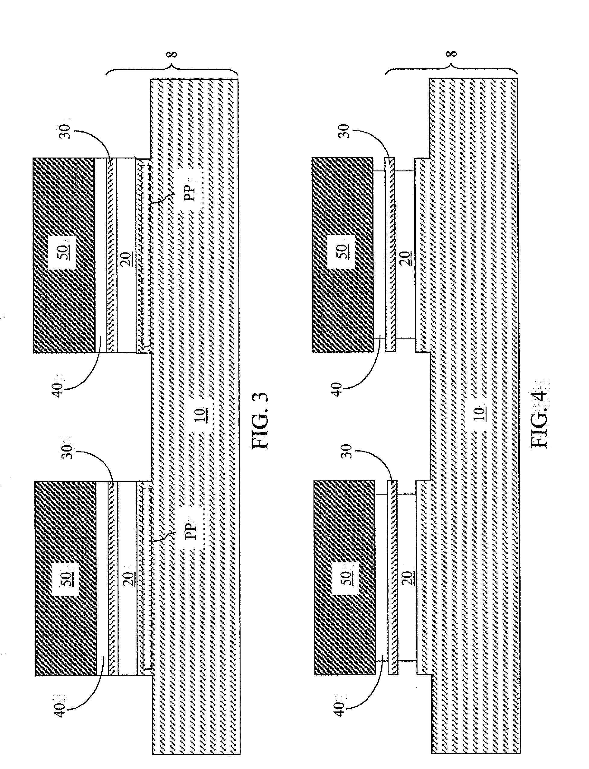
[0063]Referring to FIG. 21, a third exemplary semiconductor structure according to the present invention is derived from the second exemplary semiconductor structure of FIG. 13 by forming a dielectric oxide-containing layer 52 on exposed surfaces of the handle substrate 10 and at least one dielectric oxide-containing portion54 on exposed surfaces of each of the at least one semiconductor material portion 30. The dielectric oxide-containing layer 52 and the at least one dielectric oxide-containing portion 54 are formed without performing any lateral recessing of the at least one buried insulator portion 20 and at least one dielectric oxide portion 40. Therefore, sidewalls of the at least one buried insulator portion 20 are vertically coincident with sidewalls of the at least one semiconductor material portion 40. Preferably, the dielectric oxide-containing layer 52 does not contact the sidewalls of the at least one buried insulator portion 20.
[0064]Referring to FIG. 22, a processing ...
PUM
 Abstract
Description
Claims
Application Information