
Heterostructure for electronic power components, optoelectronic or photovoltaic components

a technology of optoelectronic or photovoltaic components and electronic power components, applied in the direction of crystal growth process, polycrystalline material growth, transportation and packaging, etc., can solve the problems of reducing the effectiveness of electronic, optical or optoelectronic devices formed on this material, difficult to manufacture with current technologies, and high cost, so as to facilitate the epitaxial growth of an active layer

Inactive Publication Date: 2011-06-02
S O I TEC SILICON ON INSULATOR THECHNOLOGIES
View PDF4 Cites 44 Cited by
  • Summary
  • Abstract
  • Description
  • Claims
  • Application Information

AI Technical Summary

Benefits of technology

[0016]The support of the present invention enables and facilitates the epitaxial growth of an active layer of a material that has a composition of AlxInyGa(1-x-y)N, where 0≦x≦1, 0≦y≦1 and x+y≦1. The heterostructure formed by growing such an active layer on the support substrate represents an embodiment of the invention as do the methods for manufacturing the support(s) and heterostructure(s).

Problems solved by technology

These substrates are, however, difficult to manufacture with current technologies and remain very expensive.
But the growth of thick layers with a good crystalline quality is still difficult with current methods if the seed substrate is not of the same material as the material epitaxied.
The epitaxy of a thick layer of GaN (approximately 10 micrometers) on a seed substrate such as doped Si or SiC, due to the differences in the coefficient of thermal expansion (CTE) and lattice parameter between the materials, leads to the formation of defects and cracks in the layer which reduces the effectiveness of the electronic, optical or optoelectronic devices formed on this material.
The epitaxy of a thick layer of GaN on a sapphire substrate followed by the transfer of the layer to a conductive substrate by laser detachment is an expensive process.
In addition, the choice of these materials does not allow a dislocation density of less than 107 cm−2 to be reached in the active layer.
In addition, the layer thus formed presents very significant bending which necessitates long preparation steps (polishing, etc.) so that it may be bonded and transferred to a final substrate.
In addition, the transfer of a layer of GaN from a bulk substrate by the Smart Cut™ technology does not enable the desired thicknesses to be reached in a satisfactory manner to date.
This method is complex since it involves two transfers of the active layer of GaN to form the final conductive structure.

Method used


Image

  • Heterostructure for electronic power components, optoelectronic or photovoltaic components
  • Heterostructure for electronic power components, optoelectronic or photovoltaic components
  • Heterostructure for electronic power components, optoelectronic or photovoltaic components

Examples


Embodiment Construction

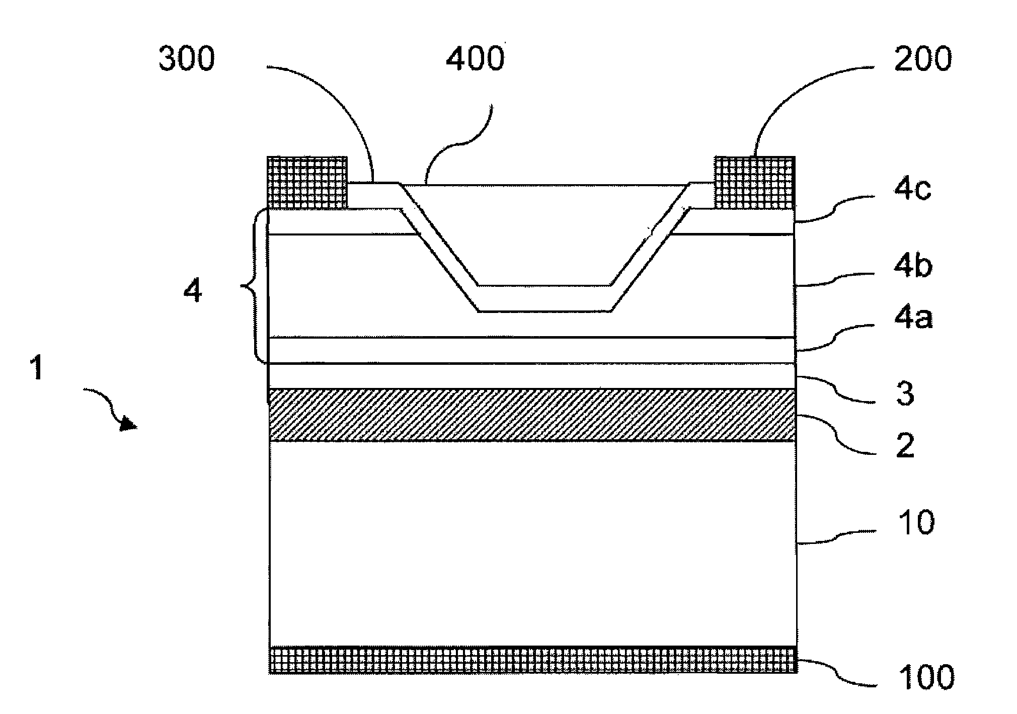
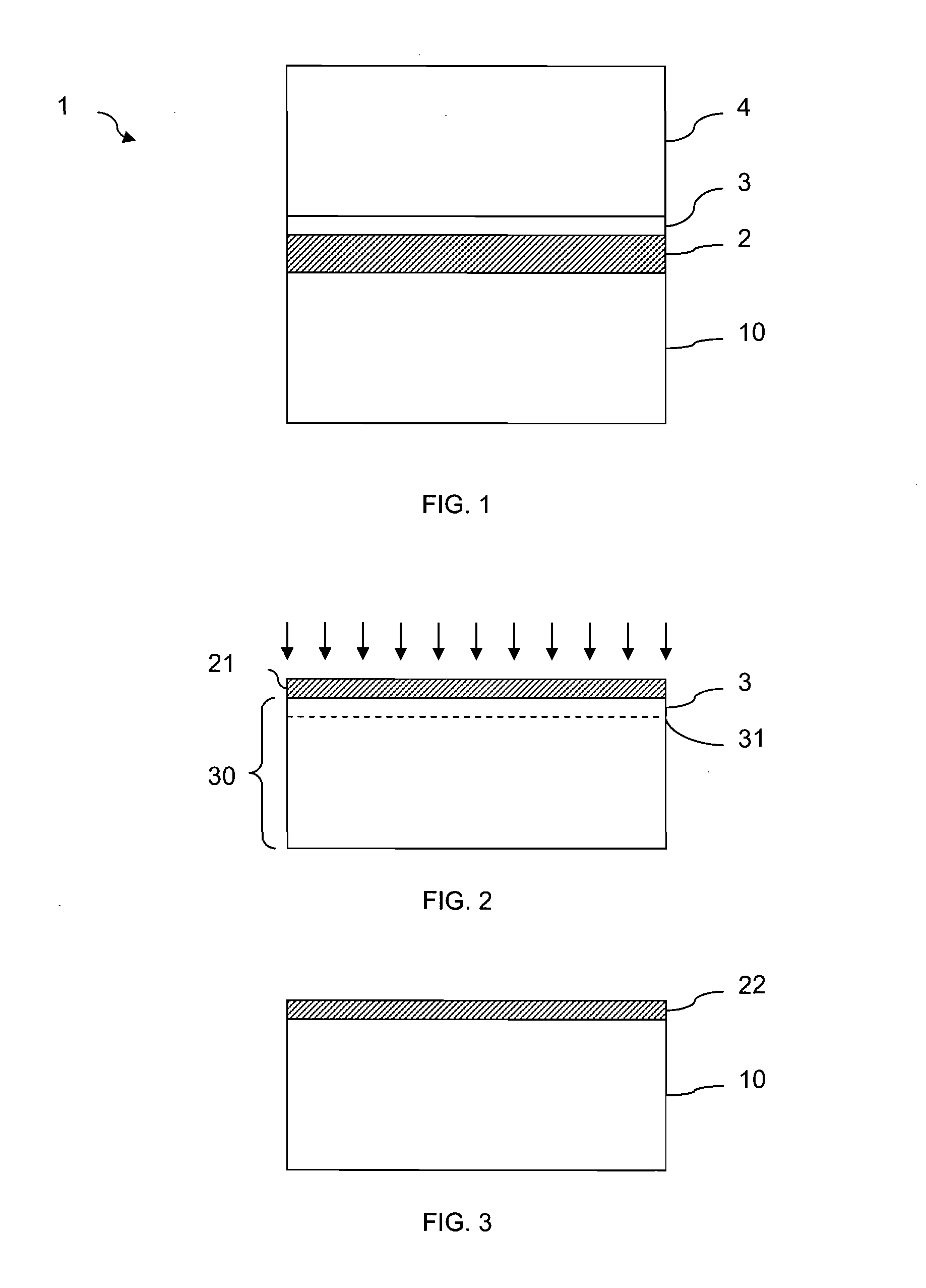
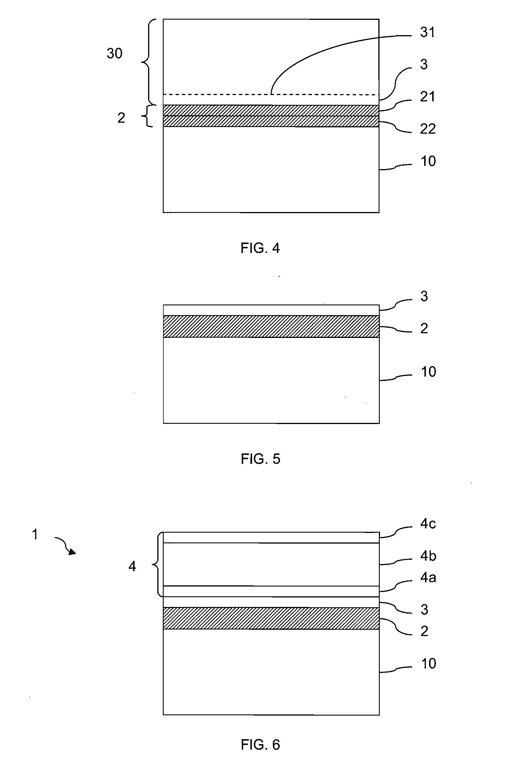
[0045]In the present text, “layer portion” is understood to refer to a part of a layer considered in the sense of the thickness of the layer. Thus, a layer may be constituted of several stacked portions, the sum of the thicknesses of portions being equal to the total thickness of the layer. The different portions of the active layer may be in the same material, but with different doping, or rather may be in different materials of composition AlxInyGa(1-x-y)N, where 0≦x≦1, 0≦y≦1 and x+y≦1. Thus, the active layer of a PIN diode may be designed with alternating InGaN / GaN / InGaN or doped p GaN / weakly doped GaN / doped n GaN layers. The active layer for optoelectronic or photovoltaic components may be constituted of a stack of layers in different materials of composition AlxInyGa(1-x-y)N, where 0≦x≦1, 0≦y≦1 and x+y≦1.

[0046]In addition, “subjacent” designates a layer portion the farthest removed from the surface of the heterostructure and “superjacent” designates a layer portion closest to t...


PUM

PropertyMeasurementUnit
Temperatureaaaaaaaaaa
Fractionaaaaaaaaaa

Abstract

The present invention relates to a support for the epitaxy of a layer of a material of composition AlxInyGa(1-x-y)N, where 0≦x≦1, 0≦y≦1 and x+y≦1, having successively from its base to its surface; a support substrate, a bonding layer, a monocrystalline seed layer for the epitaxial growth of the layer of material AlxInyGa(1-x-y)N. The support substrate is made of a material that presents an electrical resistivity of less than 10−3 ohm·cm and a thermal conductivity of greater than 100 W·m−1·K−1. The seed layer is in a material of the composition AlxInyGa(1-x-y)N, where 0≦x≦1, 0≦y≦1 and x+y≦1. The seed and bonding layers provide a specific contact resistance that is less than or equal to 0.1 ohm·cm−2, and the materials of the support substrate, the bonding layer and the seed layer are refractory at a temperature of greater than 750° C. or even greater than 1000° C. The invention also relates to methods for manufacturing the support.

Description

FIELD OF THE INVENTION[0001]The present invention relates to a support for producing a heterostructure for the manufacture of electronic power components, optoelectronic components, or photovoltaic components having a support substrate, a bonding layer, a crack-free monocrystalline layer, known as the “active layer” of a material with a composition of AlxInyGa(1-x-y)N, where 0≦x≦1, 0≦y≦1 and x+y≦1, presents a thickness of between 3 and 100 micrometers, in which or upon which the power components can be manufactured, and the methods of forming such heterostructures with or without components.BACKGROUND OF THE INVENTION[0002]For the vertical or planar electronic power device (MOS components, bipolar transistors, J-FET, MISFET, Schottky or PIN diodes, thyristors), optoelectronic component (Laser, LED) and photovoltaic component (solar cells) market, it is interesting to utilize an AlxInyGa(1-x-y)N (where x is equal to or between 0 and 1, y is equal to or between 0 and 1, where x+y is l...

Claims


Application Information

Patent Timeline
IPC IPC(8): H01L29/205C23C16/02B32B9/00B32B37/00C30B23/02
CPCH01L21/02389H01L2924/0002H01L21/187H01L33/0079H01L21/02458Y10T428/263H01L21/02658H01L21/0254H01L33/007H01L2924/00H01L33/0093
Inventor BETHOUX, JEAN-MARCLETERTRE, FABRICEWERKHOVEN, CHRISRADU, IONUTKONONCHUK, OLEG
Owner S O I TEC SILICON ON INSULATOR THECHNOLOGIES
Features
  • Generate Ideas
  • Intellectual Property
  • Life Sciences
  • Materials
  • Tech Scout
  • Unparalleled Data Quality
  • Higher Quality Content
  • 60% Fewer Hallucinations
Learn More