Solid state imaging device and electronic apparatus

a technology of solid state imaging and electronic equipment, which is applied in the direction of transistors, television systems, and scanning details of television systems, etc., can solve the problems of decreased saturation signal amount, increased variation in saturation signal amount, and inability to achieve the effect of reducing suppressing the variation of saturation signal amount, and improving image quality

Active Publication Date: 2011-06-02
SONY CORP
View PDF2 Cites 52 Cited by
  • Summary
  • Abstract
  • Description
  • Claims
  • Application Information

AI Technical Summary

Benefits of technology

[0021]According to a solid state imaging device according to the embodiment of the invention, since the potential change of the transfer gate electrode in the pixel driving period is suppressed, it is possible to suppress the variation of the saturation signal amount involved with the miniaturization of the pixel size.
[0022]According to an electronic apparatus according to the embodiment

Problems solved by technology

Therefore, the saturation signal amount is necessarily set to a low-level specification, so that there is a problem in terms of imaging characteristics.
Particularly, due to the aforementioned problem in terms of structure, the back illumination type CMOS solid stat

Method used


Image

  • Solid state imaging device and electronic apparatus
  • Solid state imaging device and electronic apparatus
  • Solid state imaging device and electronic apparatus

Examples


first embodiment

2. First Embodiment

Example of Configuration of Solid State Imaging Device

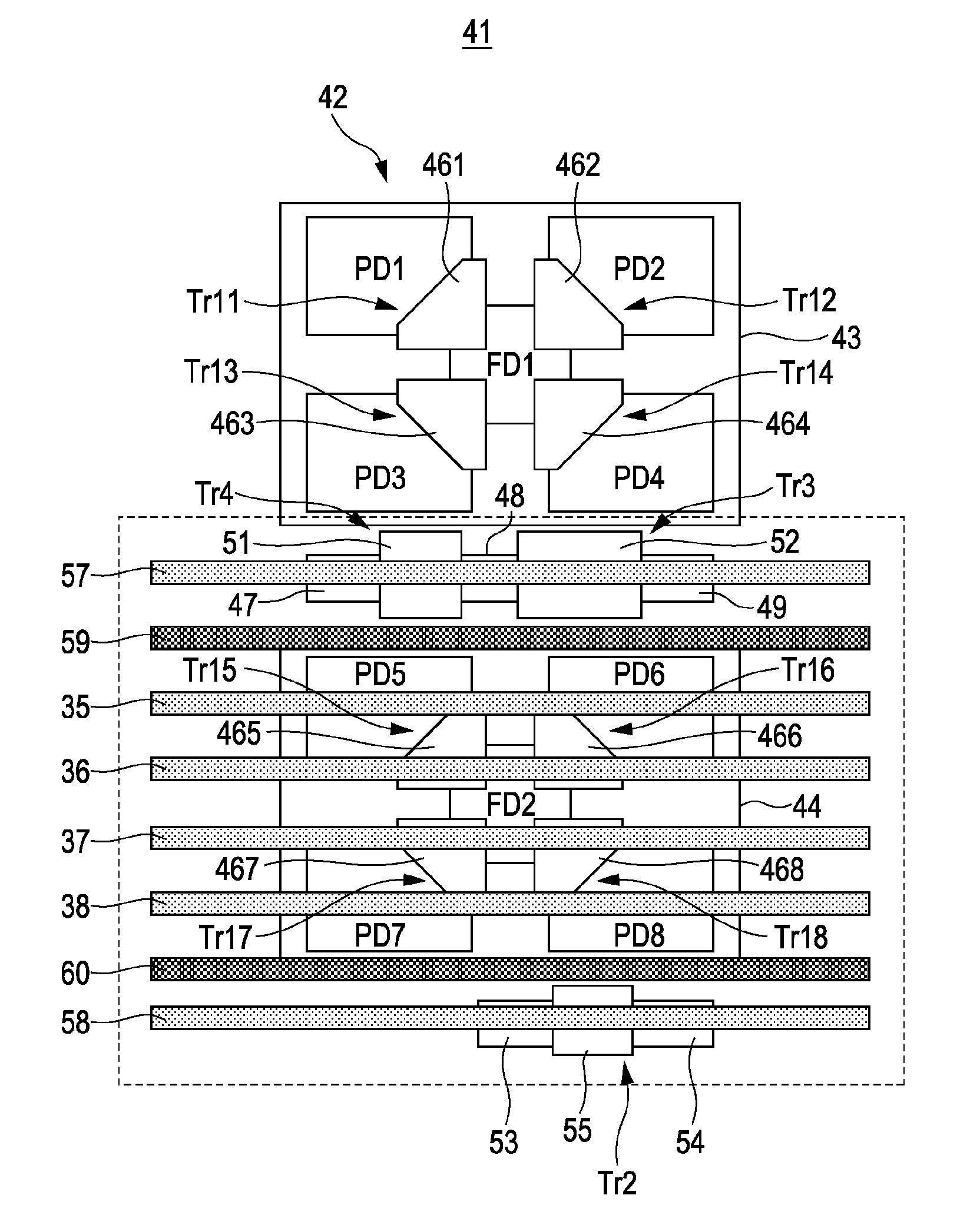
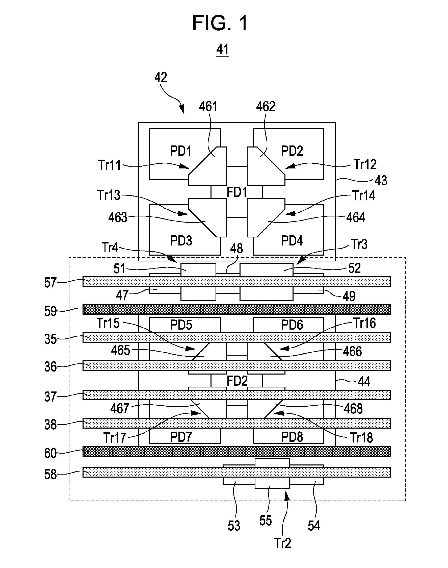
[0066]FIG. 1 illustrates a solid state imaging device according to a first embodiment of the invention. The embodiment may be adapted to a back illumination type CMOS solid state imaging device, where pixel sharing units of four pixels, eight pixels, or horizontal 2×vertical 2n (n is a positive integer, that is, n=1, 2, 3, . . . ) pixels are aligned in a two-dimensional array shape. As the pixel sharing unit, horizontal 2×vertical 2 (total four) pixels constitute one unit irrespective of the number of shared pixels. Therefore, in FIG. 1, the embodiment is described by using one unit of the horizontal 2×vertical 2 (total four) pixels.

[0067]As the solid state imaging device according to the first embodiment, a back illumination type CMOS solid state imaging device where 8-pixel sharing units are disposed in a two-dimensional array shape is adapted. In the solid state imaging device 41 according to the first embod...

second embodiment

3. Second Embodiment

Example of Configuration of Solid State Imaging Device

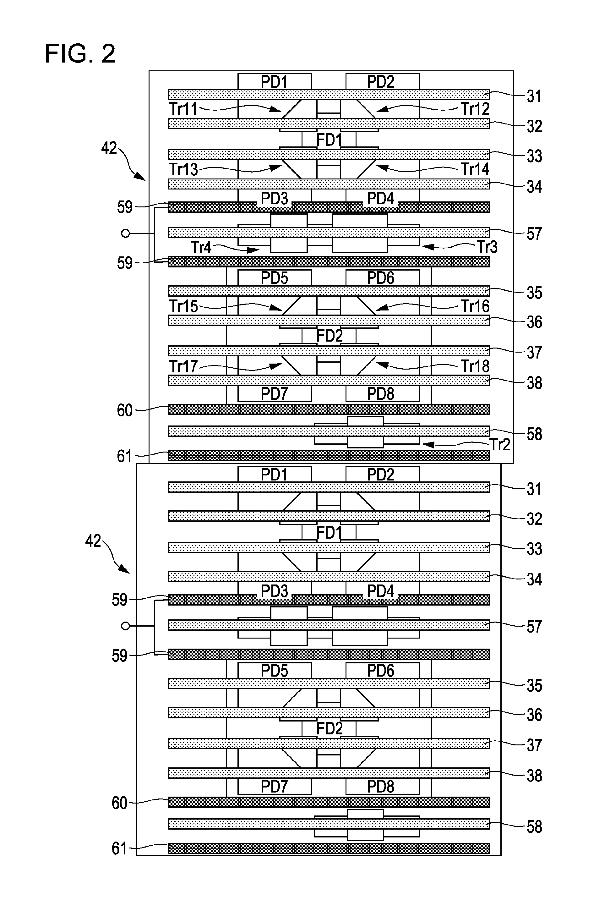
[0092]FIG. 3 illustrates a solid state imaging device according to a second embodiment of the invention. The embodiment may be adapted to a back illumination type CMOS solid state imaging device, where pixel sharing units of 4 pixels, 8 pixels or horizontal 2×vertical 2n (n is a positive integer, that is, n=1, 2, 3, . . . ) pixels are aligned in a two-dimensional array shape. As the pixel sharing unit, horizontal 2×vertical 2 (total four) pixels constitute one unit irrespective of the number of shared pixels. Therefore, similarly to FIG. 1, in FIG. 3, the embodiment is described by using one unit of the horizontal 2×vertical 2 (total four) pixels.

[0093]As the solid state imaging device according to the second embodiment, a back illumination type CMOS solid state imaging device where 8-pixel sharing units are disposed in a two-dimensional array shape is adapted. The solid state imaging device 71 according to th...

third embodiment

4. Third Embodiment

Example of Configuration of Solid State Imaging Device

[0097]FIG. 4 illustrates a solid state imaging device according to a third embodiment of the invention. The embodiment may be adapted to a back illumination type CMOS solid state imaging device, where pixel sharing units of 4 pixels, 8 pixels, or horizontal 2×vertical 2n (n is a positive integer, that is, n=1, 2, 3, . . . ) pixels are aligned in a two-dimensional array shape. As the pixel sharing unit, horizontal 2×vertical 2 (total four) pixels constitute one unit irrespective of the number of shared pixels. Therefore, similarly to FIG. 1, in FIG. 4, the embodiment is described by using one unit of the horizontal 2×vertical 2 (total four) pixels.

[0098]As the solid state imaging device 73 according to the third embodiment, a back illumination type CMOS solid state imaging device where 8-pixel sharing units are disposed in a two-dimensional array shape is adapted. In the solid state imaging device 73 according t...


PUM


Abstract

Provided is a solid state imaging device including: a pixel portion where pixel sharing units are disposed in an array shape and where another one pixel transistor group excluding transfer transistors is shared by a plurality of photoelectric conversion portions; transfer wiring lines which are connected to the transfer gate electrodes of the transfer transistors of the pixel sharing unit and which are disposed to extend in a horizontal direction and to be in parallel in a vertical direction as seen from the top plane; and parallel wiring lines which are disposed to be adjacent to the necessary transfer wiring lines in the pixel sharing unit and which are disposed to be in parallel to the transfer wiring lines as seen from the top plane, wherein voltages which are used to suppress potential change of the transfer gate electrodes are supplied to the parallel wiring lines.

Description

BACKGROUND OF THE INVENTION[0001]1. Field of the Invention[0002]The invention relates to a solid state imaging device and an electronic apparatus adapted to a camera or the like employing the solid state imaging device.[0003]2. Description of the Related Art[0004]As a solid state imaging device, there is known a CMOS solid state imaging device. Since the CMOS solid state imaging device has a low power source voltage and low power consumption, the CMOS solid state imaging device has been used for a digital still camera, a digital video camera, and various types of mobile terminals such as a mobile phone attached with a camera attached.[0005]The CMOS solid state imaging device includes a pixel portion where a plurality of pixels including photodiodes as photoelectric conversion portions and a plurality of pixel transistors are disposed in a two-dimensional array shape with regularity and a peripheral circuit portion which is disposed in the vicinity of the pixel portion.[0006]In gener...

Claims


Application Information

Patent Timeline
IPC IPC(8): H04N5/228H04N5/335
CPCH01L27/14609H01L27/14641H01L27/1464H04N5/374H01L27/14812H01L27/14887H01L27/14612H01L27/14636H01L27/14656H04N25/76H04N25/60H04N25/75
Inventor WAKANO, TOSHIFUMIKOGA, FUMIHIKO
Owner SONY CORP
Why Eureka
Try Eureka