

Nitride semiconductor crystal and its production method
a technology of nitride and semiconductor crystals, which is applied in the direction of crystal growth process, natural mineral layered products, synthetic resin layered products, etc., can solve the problems of reducing the internal quantum efficiency, generating the piezoelectric field, and reducing the external quantum efficiency of light emitting devices, so as to achieve the effect of easy production
- Summary
- Abstract
- Description
- Claims
- Application Information
AI Technical Summary
Benefits of technology
Problems solved by technology
Method used
Image

Examples
example 1
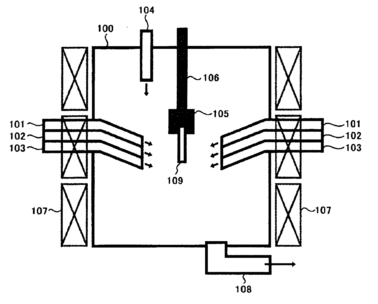
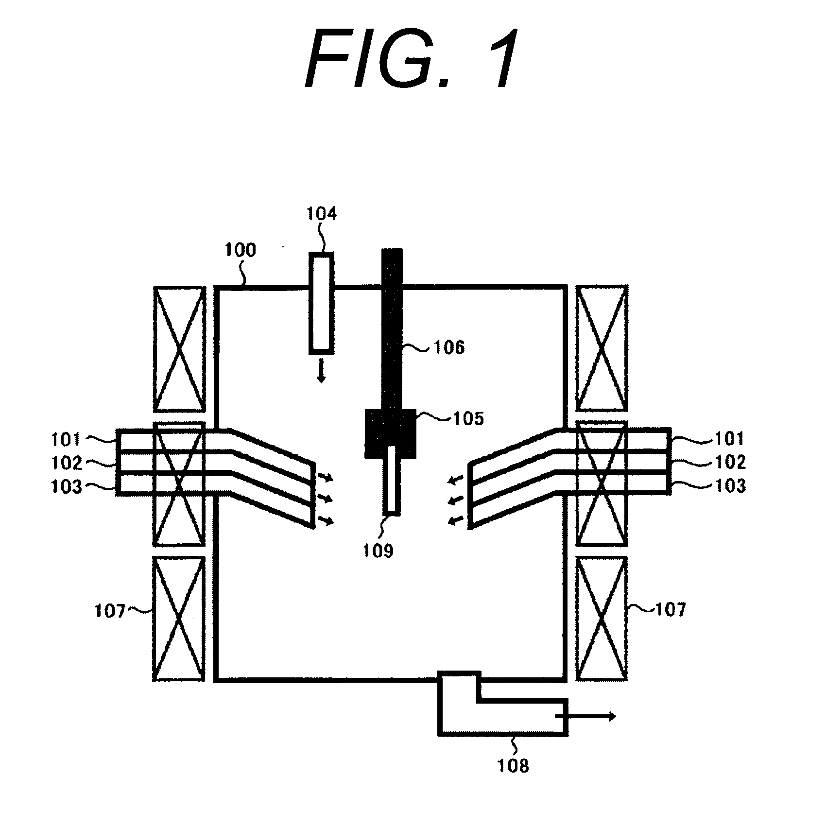
[0097]In this example, growth of a nitride semiconductor crystal was conducted using the HVPE apparatus shown in FIG. 2. The HVPE apparatus of FIG. 2 is equipped with slit-like nozzles in three stages, and a size of a first stage nozzle of a raw material feed opening is a width of 20 mm and a height of 2 mm, and is made of PBN.
[0098]GaN seed crystal 209 having M-plane as a principal plane was provided. This seed crystal is a crystal obtained by slicing a crystal prepared on C-plane GaN template with HVPE method, and is a rectangular solid having a length in a-axis direction of about 20.0 mm, a length in c-axis direction of about 8 mm and a length in m-axis direction of about 1 mm.
[0099]The seed crystal was set to a substrate holder 205 in a reactor 200 of the HVPE apparatus such that +C-plane is upward and a longitudinal direction of slit blowing opening is parallel to a-axis direction of the seed crystal. Temperature of the reactor was increased to 1,040° C., and a raw material was...
example 2
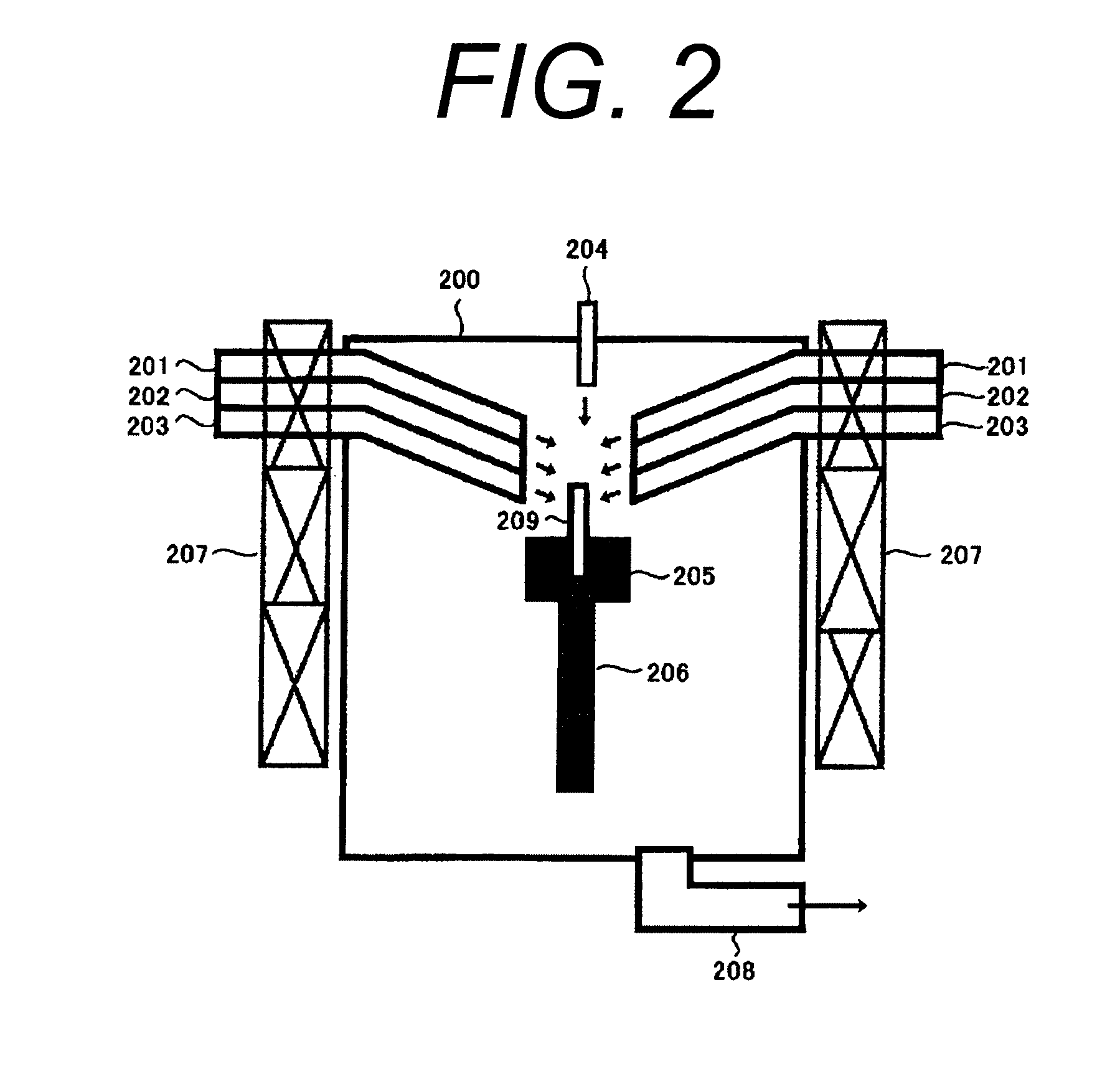
[0104]In this example, growth of a nitride semiconductor crystal was conducted using the HVPE apparatus shown in FIG. 3.
[0105]GaN seed crystal 309 having M-plane as a principal plane was provided. This seed crystal is a crystal obtained by slicing a crystal prepared on C-plane GaN template with HVPE method, and is a rectangular solid having a length in a-axis direction of about 20.0 mm, a length in c-axis direction of about 5.0 mm and a length in m-axis direction of about 0.3 mm.
[0106]The seed crystal was set to a substrate holder 305 in a reactor 300 of the HVPE apparatus such that +C-plane was upward. In this case, the -C-plane contacts with the substrate holder 305 and does not directly contact with a raw material gas.
[0107]Temperature of the reactor was increased to 1,040° C., and raw material was fed from +C-plane direction, thereby growing undoped GaN. In this growth step, growth pressure was 1.01×10⁵ Pa, partial pressure of NH3 gas was 7.03×10³ Pa, partial pressure of N2 gas ...
example 3
[0110]In this example, Example 2 was followed, except for using a rectangular solid-shaped crystal having a length in a-axis direction of about 20.0 mm, a length in c-axis direction of about 4.2 mm and a length in m-axis direction of about 4.5 mm as the GaN seed crystal.
[0111]After growing for 40 hours, temperature was decreased to room temperature. GaN single crystal obtained had a plate-like shape having a length in a-axis direction of about 22.0 mm, a length in c-axis direction of about 11.0 mm and a thickness in m-axis direction of about 5.6 mm. Area of a principal plane (M-plane) was 187.0 mm2.
[0112]The GaN single crystal was sliced, polished and shape-adjusted. Thus, five self-standing substrates each having a length in a-axis direction of 20.0 mm, a length in c-axis direction of 10.0 mm and a thickness of 330 μm and having a rectangle-shaped M-plane as a principal plane were obtained.
PUM
| Property | Measurement | Unit |
|---|---|---|
| Length | aaaaa | aaaaa |
| Length | aaaaa | aaaaa |
| Length | aaaaa | aaaaa |
Abstract
Description
Claims
Application Information