Metal base circuit board

Active Publication Date: 2011-06-09
DENKA CO LTD
View PDF6 Cites 29 Cited by
  • Summary
  • Abstract
  • Description
  • Claims
  • Application Information

AI Technical Summary

Benefits of technology

[0013]In the present invention, the problem to be solved is to improve the workability of printed circuit boards during circuit formation and during LED m

Problems solved by technology

Because of this, the deterioration of the semiconductor elements is accelerated due to the temperature rise of the LEDs, and the operating lifespan of the LEDs becomes shorter.
However, in this method, it is difficult for a printed circuit board alone to diss

Method used


Image

  • Metal base circuit board
  • Metal base circuit board

Examples


embodiment examples

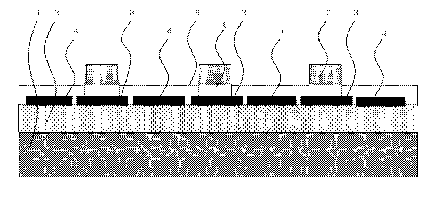
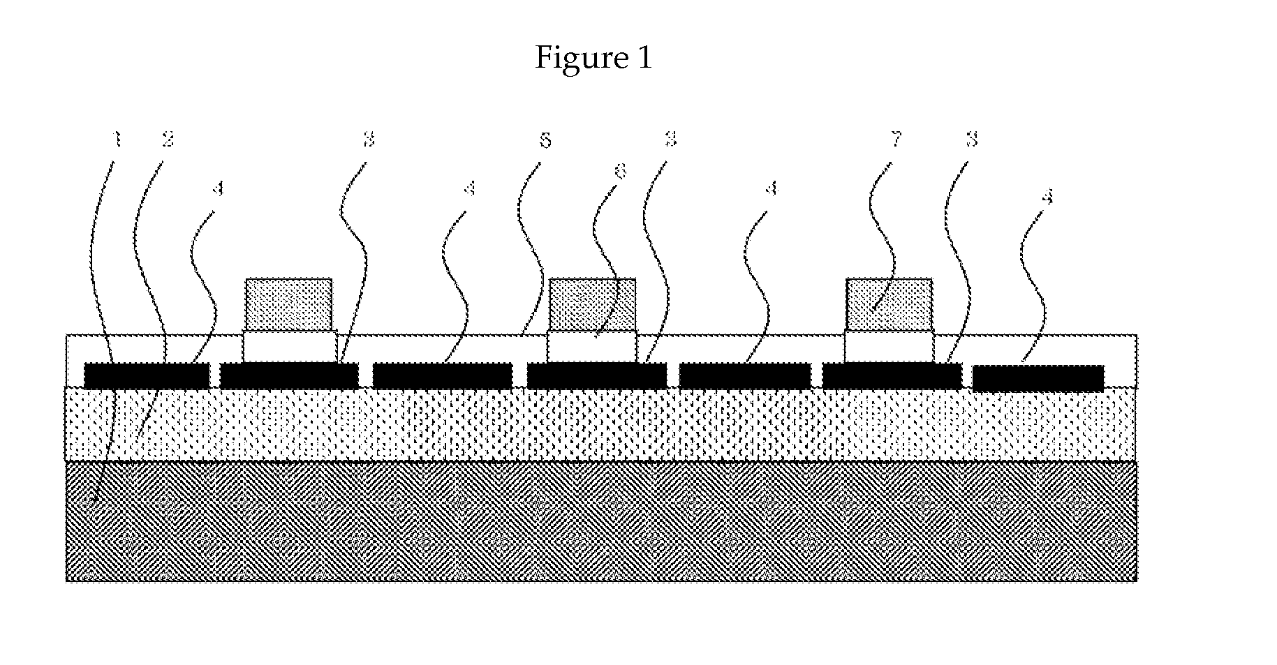
[0092]The metal base circuit board of embodiment example 1 was made according to the following method.

[0093]An insulating layer 2 was formed on a copper foil having a thickness of 35 μm, in such a way that the thickness after curing is 150 μm.

[0094]The insulating layer 2 was blended by adding, to a bisphenol A type epoxy resin (“EPICLON-828”, manufactured by Dainippon Ink and Chemicals), diaminodiphenylmethane (“H84B”, manufactured by Nihon Gosei Kako) as an amine-based curing agent, and then adding silicon oxide in the form of fragmented coarse particles having an average particle size of 1.2 μm (“A-1”, manufactured by Tatsumori) and silicon oxide in the form of fragmented coarse particles having an average particle size of 10 μm (“SQ-10”, manufactured by Hayashi Kasei) so as to form 35 percent by volume of the insulating layer (the mass ratio of spherical coarse particles and spherical fine particles being 6:4).

[0095]Next, aluminum foil of thickness 200 μm was stuck on, and the in...


PUM

PropertyMeasurementUnit
Fractionaaaaaaaaaa
Fractionaaaaaaaaaa
Percent by volumeaaaaaaaaaa

Abstract

Lifespan of LEDs can be lengthened, and the workability of the printed circuit board during circuit formation and during LED mounting can be improved.
A metal base circuit board, having an insulating layer with a linear expansion coefficient of 60 ppm per degree C. or higher and 120 ppm per degree C. or lower, a metal foil provided on one side of the insulating layer, comprising a metal material with a linear expansion coefficient of 10 ppm per degree C. or higher and 35 ppm per degree C. or lower, a circuit portion and a non-circuit potion having a linear expansion coefficient of 10 ppm per degree C. or higher and 35 ppm per degree C. or lower, and a white film formed on top of the insulating layer, circuit portion, and non-circuit portion, the total sum of the areas of the non-circuit portion and the circuit portion on top of the insulating layer being 50% or higher and 95% or lower relative to the area of the metal foil, and the relation between the linear expansion coefficients of each of the materials being: linear expansion coefficient of insulating layer>linear expansion coefficient of metal foil>linear expansion coefficient of circuit portion and non-circuit portion.

Description

CROSS-REFERENCE TO RELATED APPLICATIONS[0001]This application claims the benefit of PCT International Patent Application No. PCT / JP2009 / 059363, filed May 21, 2009, and Japanese Patent Application No. 2008-140303, filed May 29, 2008, in the Japanese Patent Office, the disclosures of which are incorporated herein by reference.BACKGROUND OF THE INVENTION[0002]1. Field of the Invention[0003]The present invention concerns a metal base circuit board for use in fields where heat dissipation and thinness are demanded, such as liquid crystal display devices that use LEDs (light emitting diodes) as light sources.[0004]2. Description of the Related Art[0005]Examples of light sources for liquid crystal backlights are CCFLs (Cold Cathode Fluorescent Lamps) and LEDs.[0006]CCFLs have ease of use and long operating lifespan as advantages, whereas LEDs have the advantages of excellent color reproduction, high brightness, and thinness, and since they do not use mercury they have a lower environmental...

Claims


Application Information

Patent Timeline
IPC IPC(8): H05K1/03H01L33/60H01L33/62H01L33/64
CPCF21K9/00Y10T428/252H01L33/46H01L33/60H05K1/0271H05K1/0274H05K1/056H05K3/0061H05K3/285H05K2201/0209H05K2201/068H05K2201/09781H05K2201/10106H05K2201/2054Y10T29/49165Y10T29/49117Y10T428/24917Y10T29/49126Y10T428/24926Y10T428/12569H01L25/0753H01L2924/0002H01L2924/00
Inventor NISHI, TAIKIMIYAKAWA, TAKESHIYAMAZAKI, KIYOKAZUSAIKI, TAKASHI
Owner DENKA CO LTD
Why Eureka
Try Eureka