Electronic Component Device and Method for Manufacturing the Same

a technology of electronic components and manufacturing methods, applied in the direction of coupling device connections, electrical apparatus casings/cabinets/drawers, soldering apparatus, etc., can solve the problems of high production cost, low productivity, and quality degradation, and achieve rapid growth rate, reduce production cost, and form in a short time

Active Publication Date: 2011-06-09
MURATA MFG CO LTD
View PDF3 Cites 55 Cited by
  • Summary
  • Abstract
  • Description
  • Claims
  • Application Information

AI Technical Summary

Benefits of technology

[0033]In accordance with the present invention, since the Ni—Bi—Au ternary alloy, or the mixed alloy of a Ni—Bi—Au ternary alloy and Au2Bi, or Au2Bi, which is formed at the bonding section, has a rapid growth rate as compared with Cu3Sn or NiBi described above, the bonding section can be formed in a short time and production cost can be reduced.
[0034]Further, in accordance with the present invention, it is possible to prevent the alloy formed at the bonding section from melting, for example, in a solder reflow step since the alloy has a high melting point of 280° C. or more. Accordingly, when the electronic component device of the present invention includes the main substrate and the cover substrate, the electronic circuit forming section and the first sealing frame surrounding the electronic circuit forming section are formed on one main surface of the main substrate, the second sealing frame to be bonded to the first sealing frame is formed on one main surface of the cover substrate and the present invention is applied for bonding the first sealing frame to the second sealing frame, the hermeticity of the electronic component device is not impaired even after the solder reflow step.
[0035]As described above, in the case where the electronic component device of the present invention includes the main substrate and the cover substrate, when the first connecting electrode is formed at a location, surrounded by the first sealing frame, on one main surface of the main substrate and a second connecting electrode is formed at a location, surrounded by the second sealing frame, on one main surface of the cover substrate, if the first connecting electrode is electrically connected to the second connecting electrode concurrently with performing a heating and bonding step on the first sealing frame and the second sealing frame, sealing and electrical connection can be achieved at one time, and therefore the number of steps for manufacturing the electronic component device can be decreased and the production cost can be reduced.
[0036]In the present invention, when the bonding section is constituted by a mixed layer of two types of alloys, a ternary alloy and Au2Bi, a strain is generated due to difference in physical properties (a coefficient of linear expansion, etc.) between the two type of alloys, and this can cause environment resistance to deteriorate, but when the bonding section is constituted by a single alloy layer, for example, a ternary alloy layer or a Au2Bi layer, environment resistance can be improved.
[0037]In the heating and bonding step carried out in the method for manufacturing an electronic component device of the present invention, when heating at a temperature of a melting point of an Au—Bi eutectic composition or higher and at a melting point of Bi or lower is carried out, a hermetically sealing state can be secured without impairing the quality of the electronic circuit forming section even in an electronic component device including an electronic circuit forming section having low heat resistance.
[0040]In the method for manufacturing an electronic component device of the present invention, when the Bi layer is formed on any one film of the first Ni film and the second Ni film and the Au layer is formed on any other film of the first Ni film and the second Ni film prior to the heating and bonding step, it is possible to attain a state in which the Bi layer and the Au layer are interposed between the first Ni film and the second Ni film by just arranging the first member and the second member in a predetermined manner in the heating and bonding step, and therefore the production steps of the electronic component device can be efficiently performed.

Problems solved by technology

Therefore, this process leads to a problem that productivity is low and production cost is high.
Further, the above-mentioned conditions may be extreme conditions of impairing the quality of the electronic circuit forming section included in the electronic component device.
Since Bi is melted at 271° C., if for example, a solder reflow step is performed on an electronic component device including such a bonding section, Bi may be melted and therefore a hermetically sealing state may be impaired.
Therefore, this process leads to a problem that productivity is low and production cost is high.

Method used


Image

  • Electronic Component Device and Method for Manufacturing the Same
  • Electronic Component Device and Method for Manufacturing the Same
  • Electronic Component Device and Method for Manufacturing the Same

Examples


first embodiment

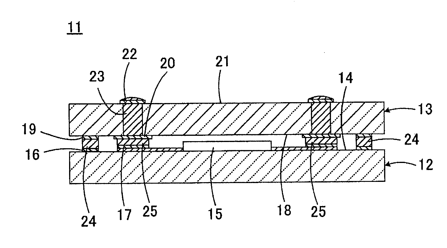
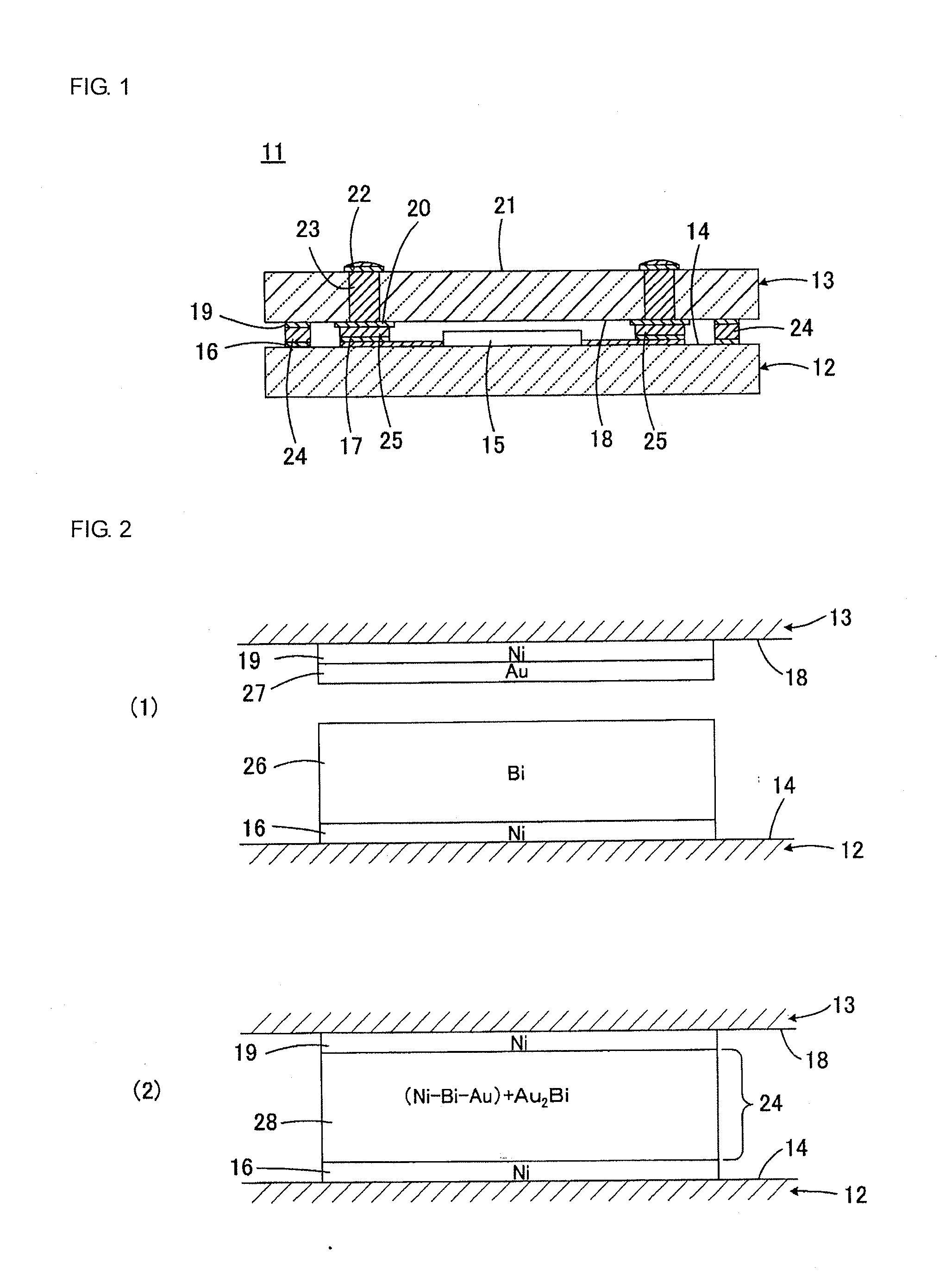
[0057]FIG. 2 is a view for illustrating the present invention and shows an enlarged view of a part of the first sealing frame 16 and a part of the second sealing frame 19 in FIG. 1. FIG. 2(1) shows a pre-bonding state and FIG. 2(2) shows a post-bonding state of the first sealing frame 16 and the second sealing frame 19.

[0058]With reference to FIG. 2(1), both of the first sealing frame 16 and the second sealing frame 19 are composed of a Ni film predominantly composed of Ni. Each of the widths of the first and second sealing frames 16 and 19 is, for example, 50 μm. In addition, in order to enhance adhesion between the Ni film and each of the main substrate 12 and the cover substrate 13, a Ti film, but not shown, may be formed between the Ni film and the main substrate 12 and between the Ni film and the cover substrate 13.

[0059]A Bi layer 26 predominantly composed of Bi is formed on the first sealing frame 16. On the other hand, an Au layer 27 predominantly composed of Au is formed on...

second embodiment

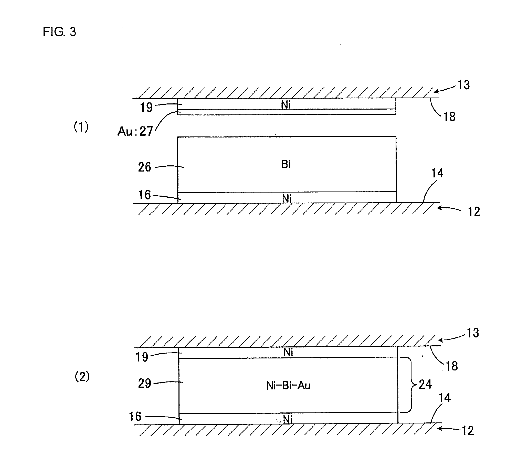
[0071]FIG. 3 is a view corresponding to FIG. 2 for illustrating the present invention. In FIG. 3, the same reference symbols are given to elements corresponding to the elements shown in FIG. 2, and overlapped descriptions are omitted.

[0072]The second embodiment has a feature that the Au layer 27, which is smaller in thickness than that in the first embodiment, is formed to avoid the formation of an Au2Bi layer at the bonding section 24. That is, the thickness of the Au layer 27 is determined in such a way that a volume of Au supplied from the Au layer 27 is 11.1% of a volume of Bi supplied from the Bi layer 26. As an example, when the thickness of the Bi layer 26 is 5 μm, the thickness of the Au layer 27 is 0.55 μ. Consequently, as shown in FIG. 3(2), only a ternary alloy layer 29 predominantly composed of a Ni—Bi—Au ternary alloy is formed at the bonding section 24 as a result of the heating and bonding step.

third embodiment

[0073]FIG. 4 is a view corresponding to FIG. 2 for illustrating the present invention. In FIG. 4, the same reference symbols are given to elements corresponding to the elements shown in FIG. 2, and overlapped descriptions are omitted.

[0074]The third embodiment has a feature that the Au layer 27, which is larger in thickness than that in the first embodiment, is formed to avoid the formation of a ternary alloy layer predominantly composed of a Ni—Bi—Au ternary alloy at the bonding section 24. That is, the thickness of the Au layer 27 is determined in such a way that a volume of Au supplied from the Au layer 27 is 27% or more of a volume of Bi supplied from the Bi layer 26. As an example, when the thickness of the Bi layer 26 is 5 μm, the thickness of the Au layer 27 is 1.35 μm or more. By setting the thickness of the Au layer 27 like this, as shown in FIG. 4(2), only an Au2Bi layer 30 is formed at the bonding section 24 in performing the heating and bonding step.

[0075]In addition, wh...


PUM

PropertyMeasurementUnit
melting pointaaaaaaaaaa
temperatureaaaaaaaaaa

Abstract

An electronic component device having a first sealing frame formed on a main substrate and a second sealing frame formed on a cover substrate, both of which are composed of a Ni film. A bonding section bonds the first sealing frame to the second sealing frame. For example, a Bi layer is formed on the first sealing frame and an Au layer is formed on the second sealing frame, and then the first sealing frame and the second sealing frame are heated at a temperature of 300° C. for 10 seconds while applying pressure in the direction in which the first sealing frame and the second sealing frame are close contact with each other to form the bonding section. The bonding section is constituted by a mixed layer predominantly composed of a mixed alloy of a Ni—Bi—Au ternary alloy and Au2Bi.

Description

CROSS REFERENCE TO RELATED APPLICATIONS[0001]The present application is a continuation of International Application No. PCT / JP2009 / 064155, filed Aug. 21, 2009, which claims priority to Japanese Patent Application No. JP2008-212470, filed Aug. 21, 2008, and Japanese Patent Application No. JP2009-027108, filed Feb. 9, 2009, the entire contents of each of these applications being incorporated herein by reference in their entirety.FIELD OF THE INVENTION[0002]The present invention relates to an electronic component device and a method for manufacturing the same, and particularly to an electronic component device having a structure of bonding conductive films to be a sealing frame to each other, for example, for hermetic sealing, and a method for manufacturing the same.BACKGROUND OF THE INVENTION[0003]Electronic component devices of interest to the present invention include, for example, a BAW filter. The BAW filter includes a main substrate provided with an electronic circuit forming sec...

Claims


Application Information

Patent Timeline
Patent Type & Authority Applications(United States)
IPC IPC(8): H01R13/46H05K3/00B32B15/01
CPCH01L23/10H01L2924/01079H03H9/1014H03H9/105Y10T29/49124H01L2924/0002Y10T428/12889Y10T428/12986H01L2924/00
Inventor HORIGUCHI, HIROKIKIMURA, YUJI
Owner MURATA MFG CO LTD
Why Eureka
Try Eureka