
Eureka
For R&D, Eureka makes reading and utilizing patents & technical documents easy.
Eureka AIR
Designed for self-driven R&D workflows. Generate viable solutions, solve complex R&D challenges, empower your innovation with AI.

Eureka Materials
Designed for material experts only. Revolutionize your material R&D, from search, analyze, to developing new materials.

TechResearch
Generate reliable direction feasibility study reports for your R&D in just a few steps.

TechSeek
Discover and master advanced knowledge NOW. Basics, ideas, possibilities, all at once.

TechMind
As an expert in R&D Theories, TechMind can generates customized viable solutions instantly.

TechRisk
Analyze your overall solution with one click, know your potential R&D risks in advance.

TechMonitor
Get weekly tech updates, stay abreast of the latest tech innovations and key insights.
Radiation sensor and radiation image detection apparatus
- Summary
- Abstract
- Description
- Claims
- Application Information
AI Technical Summary
Problems solved by technology
Method used
Image

Examples
Embodiment Construction
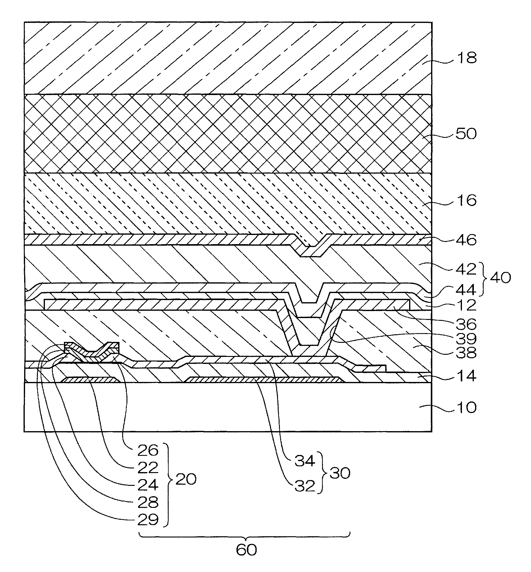
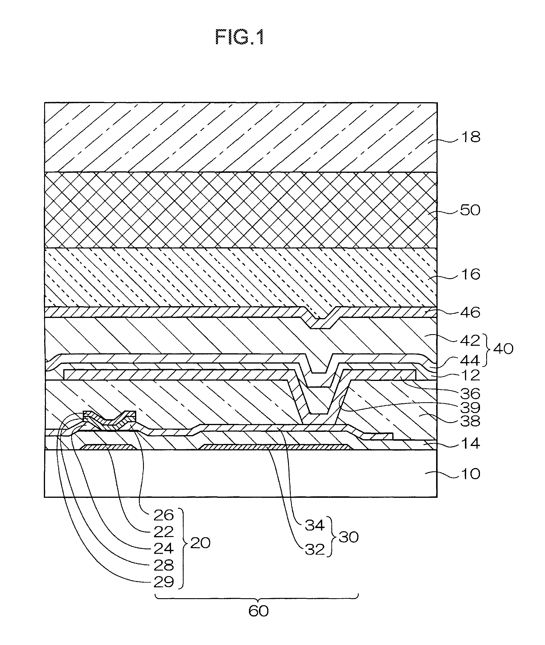
[0014]FIG. 1 is a cross-sectional view schematically illustrating the configuration of one pixel unit of a radiation sensor related to an exemplary embodiment of the radiation sensor according to the invention. In FIG. 1, a phosphor layer 50 which, when an imaging target as an object of imaging is exposed to radiation, converts the radiation that has transmitted into the imaging target, into light, is provided on one of the surfaces of a plastic support 18 such as a polyethylene terephthalate support.
[0015]Furthermore, the radiation sensor has a charge detection layer 60 which includes a storage capacitor 30 and a thin film transistor 20, on one of the surfaces of an insulating substrate 10. The storage capacitor 30 is constituted of a upper storage capacitor electrode 34 and a lower storage capacitor electrode 32, and a dielectric layer 14 disposed between these electrodes (this dielectric layer 14 also functions as an insulating film). Furthermore, this thin film transistor 20 has...
PUM
 Abstract
Description
Claims
Application Information
 - R&D Engineer
- R&D Manager
- IP Professional
- Industry Leading Data Capabilities
- Powerful AI technology
- Patent DNA Extraction
Browse by: Latest US Patents, China's latest patents, Technical Efficacy Thesaurus, Application Domain, Technology Topic, Popular Technical Reports.
© 2024 PatSnap. All rights reserved.Legal|Privacy policy|Modern Slavery Act Transparency Statement|Sitemap|About US| Contact US: help@patsnap.com