
Photovoltaic cell manufacturing method and photovoltaic cell manufacturing apparatus

Inactive Publication Date: 2011-06-09
ULVAC INC
View PDF6 Cites 3 Cited by
  • Summary
  • Abstract
  • Description
  • Claims
  • Application Information

AI Technical Summary

Benefits of technology

[0032]According to the photovoltaic cell manufacturing method of the first aspect of the present invention, the actual size per one pixel is calculated every time based on the predetermined actual size value (actual value) which is preliminarily stored in the memory and the number of pixels constituting the actual size value, even in a case where the distance between the capturing section and the photovoltaic cell varies for each production lot of photovoltaic cells due to a slight difference in thickness or the like, or the actual size per one pixel on the image varies due to an increase in the capturing magnification ratio for improvement of the degree of detection accuracy of the structural defect.
[0033]For this reason, it is not necessary for a step requiring time and effort in which the actual size per one pixel is freshly calculated for each production lot of photovoltaic cells or every changing capturing magnification ratio, thereafter, a stage is transferred and the position which is irradiated with laser light is adjusted; the length of time required for a step for repairing a defect of photovoltaic cells is eliminated, and it is possible to significantly increase the efficiency in the repairing step.
[0034]Also, since it is not necessary to form a laser vestige used for marking on the compartment element of the photovoltaic cell every calculating of the actual size per one pixel, it is possible to manufacture a photovoltaic cell having a high level of power generation efficiency without unnecessary damage to a compartment element.
[0035]Additionally, according to the photovoltaic cell manufacturing apparatus of the second aspect of the present invention, since it is not necessary to form a laser vestige used for marking on the compartment element of the photovoltaic cell every calculating of the actual size per one pixel, it is possible to manufacture a photovoltaic cell having a high level of power generation efficiency without unnecessary damage to a compartment element.

Problems solved by technology

However, in contrast, in the photovoltaic cell in which the silicon single crystal is utilized, a silicon single crystal ingot is sliced, and a sliced silicon wafer is used in the photovoltaic cell; therefore, a large amount of energy is spent for manufacturing the ingot, and the manufacturing cost is high.
Specifically, at the moment, in a case of realizing a photovoltaic cell having a large area which is placed out of doors or the like, when the photovoltaic cell is manufactured by use of a silicon single crystal, the cost considerably increases.
In the amorphous silicon photovoltaic cell that is provided with a photoelectric converter constituted of the foregoing upper and lower electrodes and the semiconductor film, the difference in the electrical potentials is small if each of the layers having a large area is only uniformly formed on the substrate, and there is a problem in that the resistance increases.
However, in the amorphous silicon photovoltaic cell having the foregoing structure, it is known that several structural defects occur during a manufacturing step therefor.
In the photoelectric converter as mentioned above, when structural defects occur such that the upper electrode and the lower electrode are locally short-circuited with the semiconductor film interposed therebetween, the defects cause malfunction such that power generation voltage or photoelectric conversion efficiency are degraded.
In addition, since it is necessary to form a laser vestige that becomes a marking on a compartment element of the photovoltaic cell every calculating of the actual size per one pixel, there is a problem in that unnecessary damage is imparted to the compartment element.

Method used


Image

  • Photovoltaic cell manufacturing method and photovoltaic cell manufacturing apparatus
  • Photovoltaic cell manufacturing method and photovoltaic cell manufacturing apparatus
  • Photovoltaic cell manufacturing method and photovoltaic cell manufacturing apparatus

Examples


Embodiment Construction

[0045]Hereinafter, the best mode of a photovoltaic cell manufacturing method and a photovoltaic cell manufacturing apparatus used therefor related to the present invention will be described with reference to drawings.

[0046]The embodiment is specifically explained for appropriate understanding of the scope of the present invention.

[0047]The technical scope of the invention is not limited to the embodiments described below, but various modifications may be made without departing from the scope of the invention.

[0048]In the respective drawings used in the explanation described below, in order to make the respective components be of understandable size in the drawing, the dimensions and the proportions of the respective components are modified as needed compared with the real components.

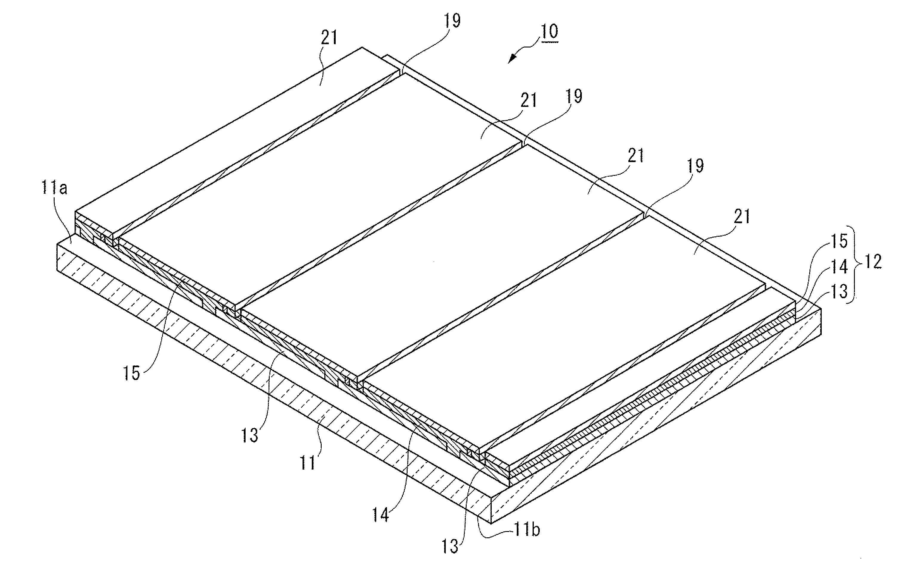
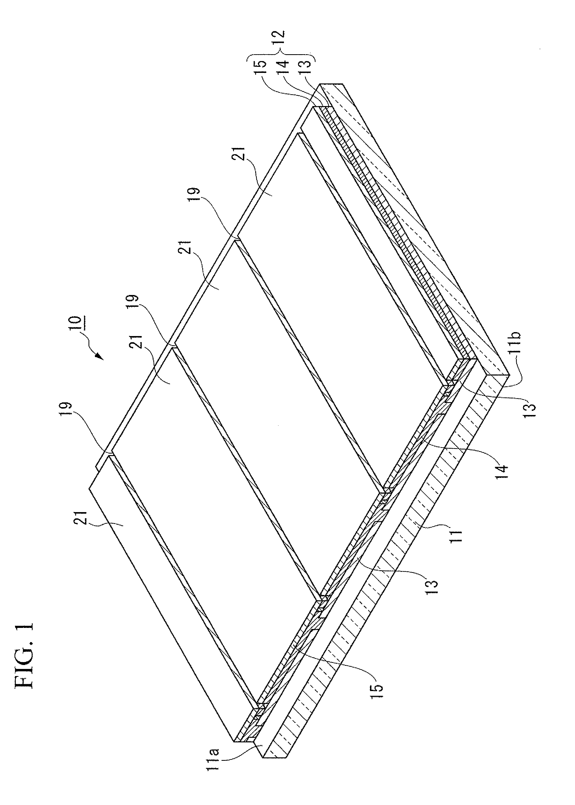
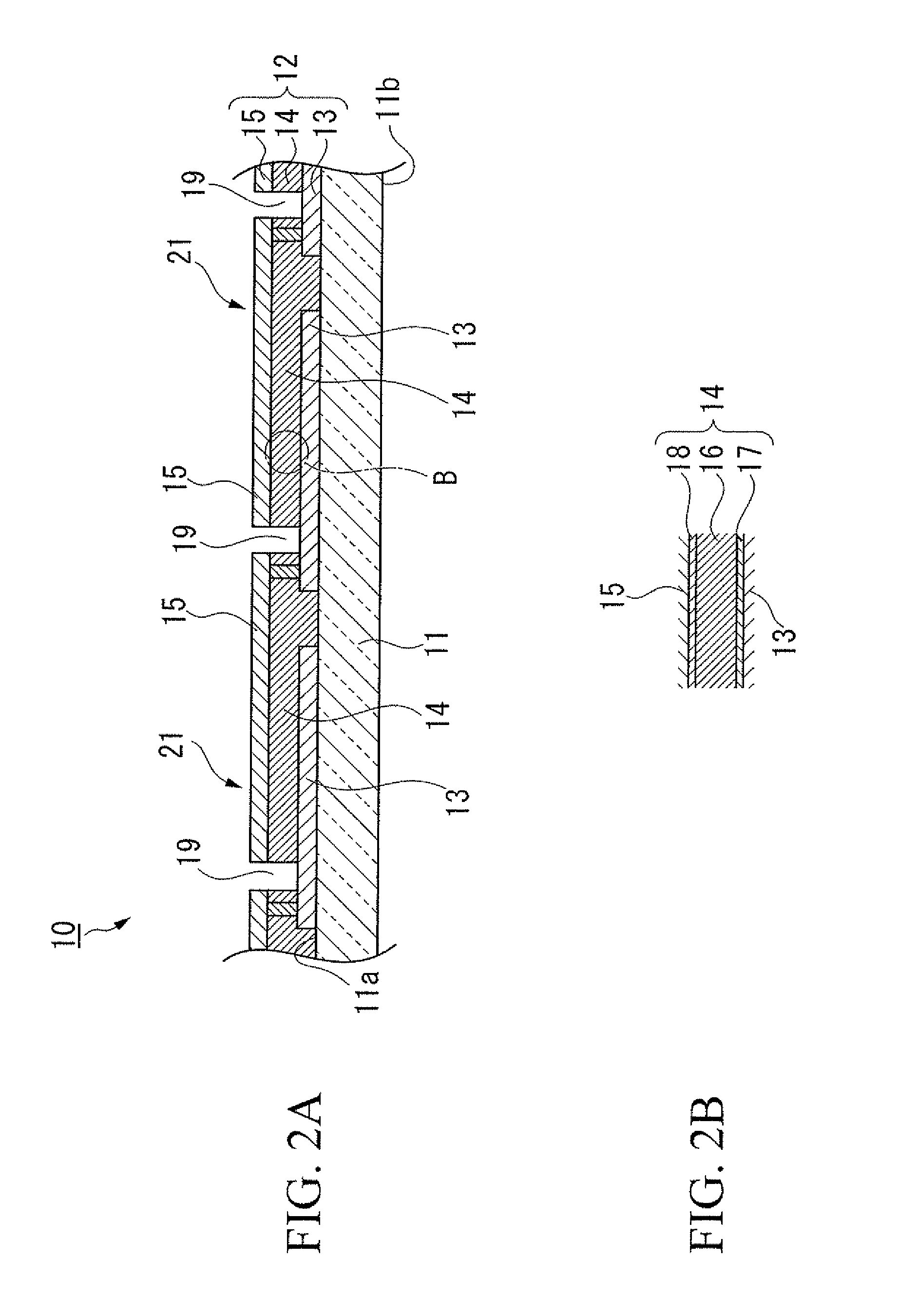
[0049]FIG. 1 is an enlarged perspective view showing an example of a main section of an amorphous silicon type photovoltaic cell which is manufactured by a method for manufacturing a photovoltaic cell of...


PUM


Abstract

A photovoltaic cell manufacturing method includes: detecting a structural defect existing in compartment elements; obtaining an image by capturing a region including the structural defect and the scribe line with a predetermined definition; specifying first number of pixels on the image, the first number of pixels corresponding to a distance between the scribe lines adjacent to each other or corresponding to a width of the scribe line; referring to an actual value indicating the distance between the scribe lines adjacent to each other or indicating the width of the scribe line, the distance being preliminarily stored, and the width of the scribe line being preliminarily stored; calculating an actual size of one pixel on the image by comparing the first number of pixels with the actual value; specifying second number of pixels on the image, the second number of pixels corresponding to the distance between the structural defect and the scribe line; comparing the second number of pixels with the actual size of one pixel, thereby calculating defect position information; and electrically separating the structural defect by irradiation with the laser light based on the defect position information.

Description

BACKGROUND OF THE INVENTION[0001]1. Field of the Invention[0002]The present invention relates to a photovoltaic cell manufacturing method and a photovoltaic cell manufacturing apparatus, and specifically relates to a photovoltaic cell manufacturing method and a photovoltaic cell manufacturing apparatus that are capable of quickly detecting and repairing a structural defect at a low cost.[0003]This application claims priority from Japanese Patent Application No. 2008-209209 filed on Aug. 15, 2008, the contents of which are incorporated herein by reference in their entirety.[0004]2. Background Art[0005]In recent years, in view of efficient use of energy, photovoltaic cells have been more widely used than ever before.[0006]Specifically, a photovoltaic cell in which a silicon single crystal is utilized has a high level of energy conversion efficiency per unit area.[0007]However, in contrast, in the photovoltaic cell in which the silicon single crystal is utilized, a silicon single cryst...

Claims


Application Information

Patent Timeline
IPC IPC(8): G06K9/00H01L21/66
CPCH01L31/208H01L31/046H02S50/10Y02E10/50Y02P70/50H01L31/04H01L31/18H01L22/00
Inventor YAMAMURO, KAZUHIROYUYAMA, JUNPEIYAMANE, KATSUMI
Owner ULVAC INC
Features
  • Generate Ideas
  • Intellectual Property
  • Life Sciences
  • Materials
  • Tech Scout
  • Unparalleled Data Quality
  • Higher Quality Content
  • 60% Fewer Hallucinations
Learn More