Method for manufacturing lamination type semiconductor integrated device

a semiconductor integrated device and lamination technology, applied in semiconductor devices, semiconductor/solid-state device details, electrical devices, etc., can solve the problems of difficult mass production, further reduction of wiring resistance in view of distance reduction among wirings,

Active Publication Date: 2011-06-09
SHIN ETSU CHEM IND CO LTD
View PDF1 Cites 52 Cited by
  • Summary
  • Abstract
  • Description
  • Claims
  • Application Information

AI Technical Summary

Benefits of technology

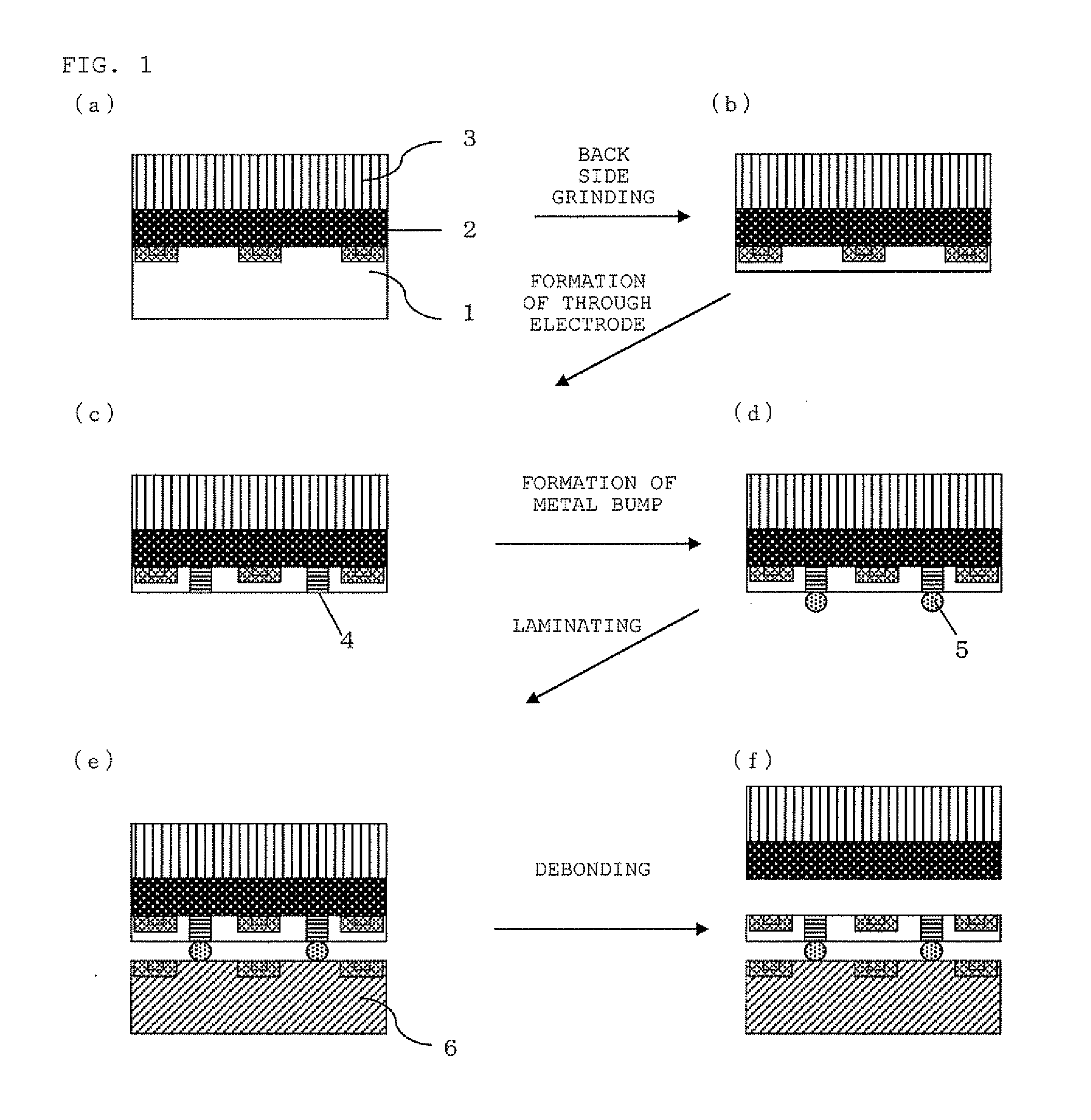
[0015]The present invention was made in view of the above-mentioned problems, and has an object to provide a method for manufacturing a lamination type semiconductor integrated device that can simultaneously satisfy grinding force resistance during back side grinding of a semiconductor wafer, heat resistance during anisotropic dry etching and the like, chemical resistance during plating and etching, smooth debonding of a support substrate for processing at the end, and low adherend staining.

Problems solved by technology

However, due to increasing speed of a device and miniaturization of a mounting device, further minuter packaging area, higher integration, and further reduction of wiring resistance in view of distance reduction among wirings is required.
CoC and CoW have a high possibility of producing a product without defect, because a semiconductor integrated device chip without defect can be selected individually and a lamination type semiconductor integrated device is produced after laminating these chips without defect; on the other hand, CoC and CoW have such problems that: position accuracy at the time of laminating is necessary in each of semiconductor integrated devices because of miniaturization of the chip size and mass production is difficult because each chip is laminated sequentially.
However, these adhesives are weak to heat, thereby leading to cause a problem that they are melted during heating process in the step of laminating by electrical bonding as mentioned above.

Method used


Image

  • Method for manufacturing lamination type semiconductor integrated device
  • Method for manufacturing lamination type semiconductor integrated device
  • Method for manufacturing lamination type semiconductor integrated device

Examples


example 1

[0130]Into a mixture solution, comprised of 40 parts by mass of vinyl-containing polydimethylsiloxane, whose both terminals of the molecular chain were blocked with an SiMe2Vi group, containing 7.5% by mole of a vinyl group and having viscosity of 22,000 mPa·s (viscosity of its 30%-toluene solution), 100 parts by mass of 60%-toluene solution of polysiloxane comprised of a Me3SiO0.5 unit and an SiO2 unit (Me3SiO0.5 / SiO2=0.80), and 26.7 parts by mass of toluene, were added 7.8 parts by mass of the crosslinking agent shown by the following formula (F), and 0.1 parts by mass of ethynyl cyclohexanol, and they were mixed.

Me3SiO—[MeHSiO]40—SiMe3  (F)

[0131](Wherein Me indicates a methyl group and Vi indicates a vinyl group.)

[0132]Into 100 parts by mass of the resulting mixture were added 50 parts by mass of toluene and 0.5 parts by mass of a platinum catalyst CAT-PL-50T (manufactured by Shin-Etsu Chemical Co., Ltd.); the mixture thus obtained was further mixed to obtain a solution of a pres...

example 2

[0133]Into a mixture solution, comprised of 70 parts by mass of vinyl-containing polydimethylsiloxane, whose both terminals of the molecular chain were blocked with an SiMe2Vi group, containing 3% by mole of a vinyl group and having viscosity of 22,000 mPa·s (viscosity of its 30%-toluene solution), 50 parts by mass of 60%-toluene solution of polysiloxane comprised of a Me3SiO0.5 unit and an SiO2 unit (Me3SiO0.5 / SiO2=0.80), and 46.7 parts by mass of toluene, were added 5.4 parts by mass of the crosslinking agent (F) and 0.1 parts by mass of ethynyl cyclohexanol, and they were mixed.

[0134]Into 100 parts by mass of the resulting mixture were added 50 parts by mass of toluene and 0.5 parts by mass of a platinum catalyst CAT-PL-50T (manufactured by Shin-Etsu Chemical Co., Ltd.); the mixture thus obtained was further mixed to obtain a solution of a pressure-sensitive silicone adhesive composition containing approximately 40% of the siloxane component. A pressure-sensitive silicone adhesiv...

example 3

[0135]Into a mixture solution, comprised of 90 parts by mass of vinyl-containing polydimethylsiloxane, whose both terminals of the molecular chain were blocked with an SiMe2Vi group, containing 3% by mole of a vinyl group and having viscosity of 22,000 mPa·s (viscosity of its 30%-toluene solution), 16.7 parts by mass of 60%-toluene solution of polysiloxane comprised of a Me3SiO0.5 unit and an SiO2 unit (Me3SiO0.5 / SiO2=0.80), and 60 parts by mass of toluene, were added 6.9 parts by mass of the crosslinking agent (F) and 0.1 parts by mass of ethynyl cyclohexanol, and they were mixed.

[0136]Into 100 parts by mass of the resulting mixture were added 50 parts by mass of toluene and 0.5 parts by mass of a platinum catalyst CAT-PL-50T (manufactured by Shin-Etsu Chemical Co., Ltd.); the mixture thus obtained was further mixed to obtain a solution of a pressure-sensitive silicone adhesive composition containing approximately 40% of the siloxane component. A pressure-sensitive silicone adhesiv...


PUM


Abstract

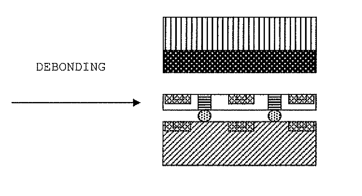
Provided is a method for manufacturing a lamination type semiconductor integrated device that can simultaneously attain grinding force resistance during back side grinding of a semiconductor wafer, heat resistance during anisotropic dry etching and the like, chemical resistance during plating and etching, smooth debonding of a support substrate for processing at the end, and low adherend staining; the method comprises at least a step of back side grinding of a first semiconductor wafer having a device formed on its surface and a step of laminating by electrical bonding the first semiconductor wafer with a second semiconductor wafer having a device formed on its surface, wherein, at the time of back side grinding of the first semiconductor wafer, back of the first semiconductor wafer is ground after surface of formed device on the first semiconductor wafer is bonded to a support substrate for processing by using a pressure-sensitive silicone adhesive.

Description

BACKGROUND OF THE INVENTION[0001]1. Field of the Invention[0002]The present invention relates to a method for manufacturing a lamination type semiconductor integrated device, in particular to a method for manufacturing a lamination type semiconductor integrated device in a wafer level using a TSV (Through Silicon Via) technology.[0003]2. Description of the Related Art[0004]A semiconductor integrated device is used in large quantity for industrial goods and so on. However, due to increasing speed of a device and miniaturization of a mounting device, further minuter packaging area, higher integration, and further reduction of wiring resistance in view of distance reduction among wirings is required.[0005]In order to realize further minuter packaging area, higher integration, and distance reduction among wirings, an investigation is being carried out to integrate a plurality of packages into one package in a semiconductor integrated device and the result has been practically used.[0006...

Claims


Application Information

Patent Timeline
Patent Type & Authority Applications(United States)
IPC IPC(8): H01L21/762
CPCH01L21/6835H01L2924/014H01L21/76898H01L23/544H01L24/81H01L25/0657H01L25/50H01L2221/6834H01L2223/54433H01L2223/54473H01L2224/11003H01L2224/81001H01L2224/81801H01L2225/06513H01L2225/06541H01L2924/01013H01L2924/01029H01L2924/01051H01L2924/01079H01L2924/01082H01L2924/01005H01L2924/01006H01L2924/01033H01L2924/01047H01L2924/0105H01L2924/01067H01L2924/01074H01L2924/01075H01L2924/01078H01L21/6836H01L2221/68327H01L2924/14H01L2924/15788
Inventor KURODA, YASUYOSHIKONDO, KAZUNORIKATO, HIDETO
Owner SHIN ETSU CHEM IND CO LTD
Why Eureka
Try Eureka