

Molecular precursor methods and articles for optoelectronics
a technology of optoelectronics and precursors, applied in the field of optoelectronics, can solve the problems of lack of uniformity of cigs layers, complex cigs materials, and limited use of optoelectronic or solar cell products, and achieve the effect of improving processability for solar cell production
- Summary
- Abstract
- Description
- Claims
- Application Information
AI Technical Summary
Benefits of technology
Problems solved by technology
Method used
Image

Examples
example 1
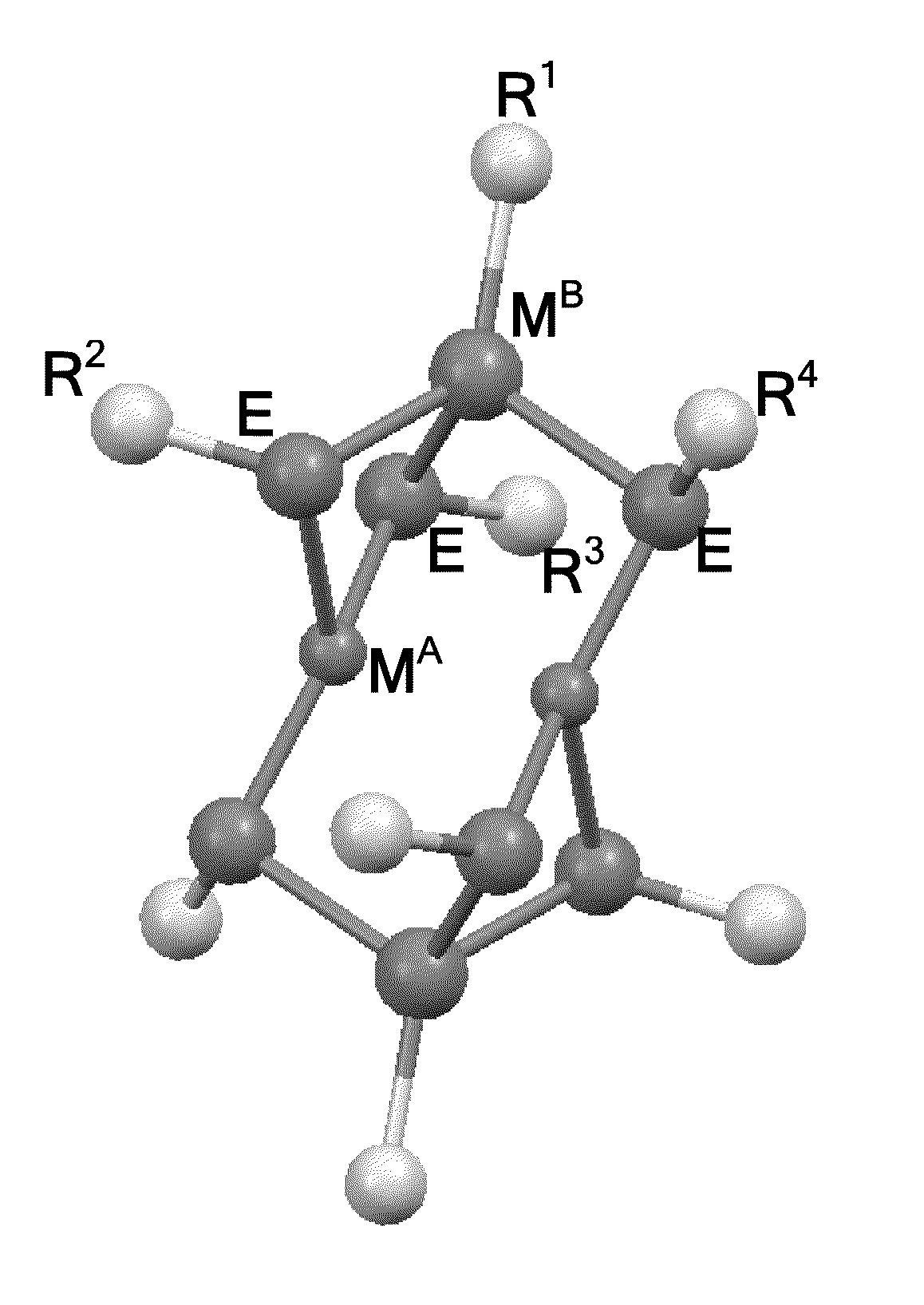
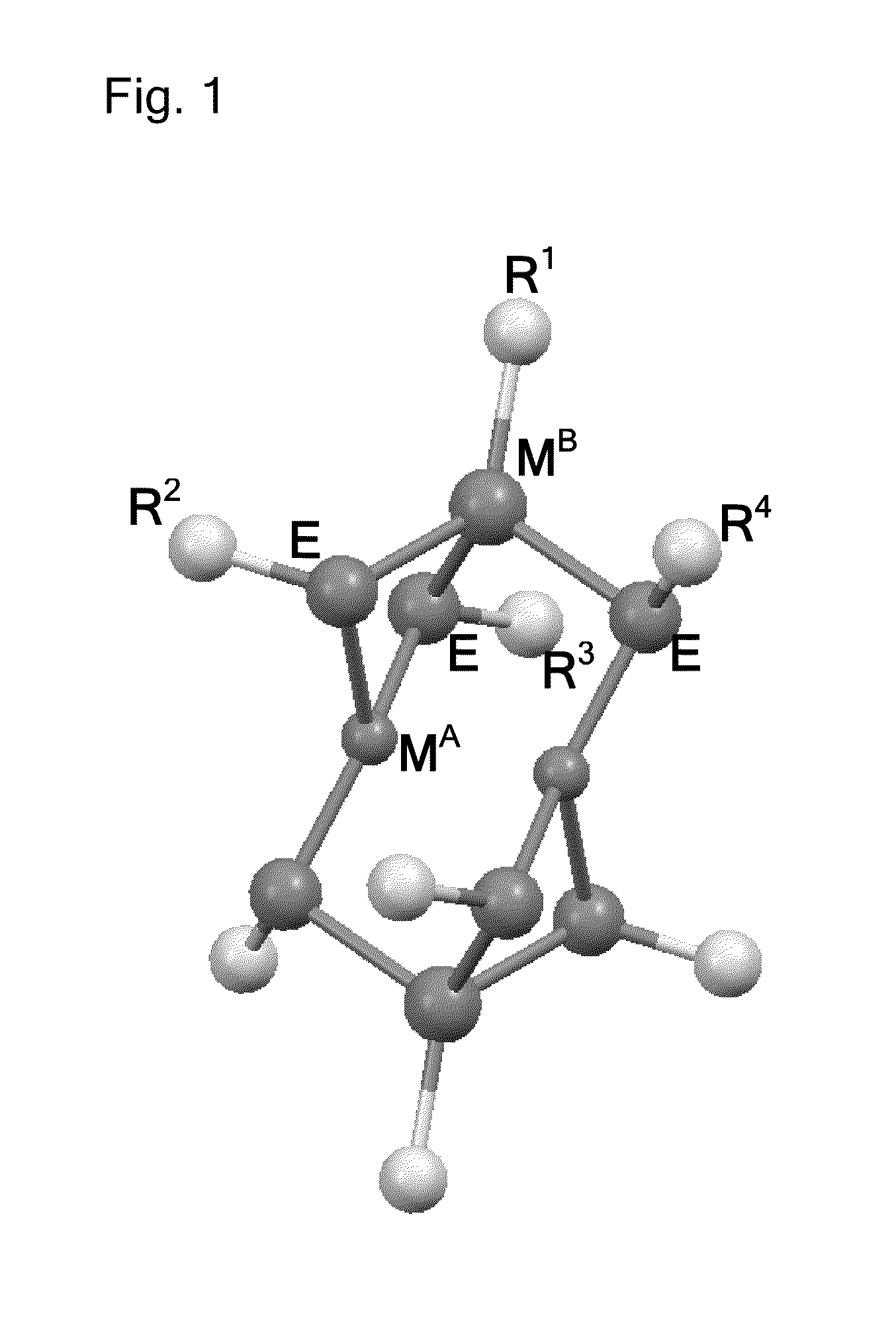
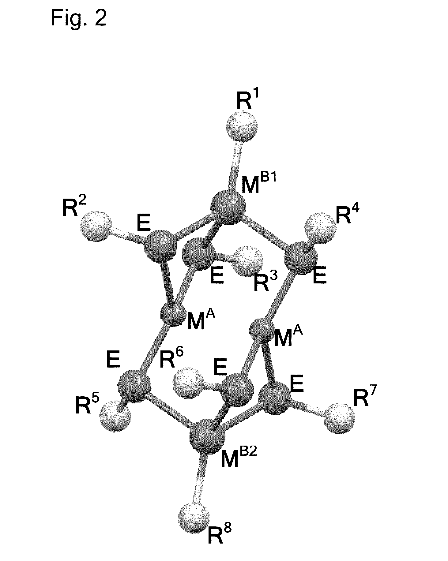
Molecular Precursor Compounds
[0455]An MP1 molecular precursor represented by the formula Cu—(StBu)3IniPr was synthesized using the following procedure. A 100 mL Schlenk tube was charged with iPr2In(StBu) (1.68 g, 6.1 mmol) and Cu(StBu) (0.93 g, 6.1 mmol) in an inert atmosphere glovebox. To this mixture was added 20 mL of dry toluene via cannula transfer using a Schlenk line. The mixture was heated until it became homogeneous. One equivalent of HStBu (0.7 mL, 6.1 mmol) was added via syringe and the Schlenk tube was kept under static N2. The mixture was heated for about 12-14 h at 60° C. with stirring. The solution was then filtered warm and crystals began to form at room temperature. The solution was cooled at −60° C. for 16 hours. Yellow crystalline solid was isolated, 1.4 g, yield 47%. Elemental analysis: C, 36.2; H, 6.7; Cu, 13.0; In, 23.9; S, 18.0. NMR: (1H) 1.66 (br s 34H); (13C) 23.15 (s); 26.64 (s); 37.68 (s); 47.44 (s). Solubility: pentane, nil; diethyl ether, ss, benzene, s ...
example 2
[0460]An MP1 molecular precursor represented by the formula Cu—(StBu)3InnBu was synthesized using the following procedure. A 100 mL Schlenk tube was charged with nBu2In(StBu) (1.8 g, 5.8 mmol) and Cu(StBu) (0.89 g, 5.8 mmol) in an inert atmosphere glovebox. To this mixture was added 20 mL of dry toluene via cannula transfer using a Schlenk line. The mixture was heated until it became homogeneous. One equivalent of HStBu (0.65 mL, 5.8 mmol) was added via syringe and the Schlenk tube was kept under static N2. The mixture was heated for about 12-14 hours at 100° C. with stirring. The solution was then allowed to cool to room temperature and filtered. The solvent was removed under vacuum, and the product was extracted with pentane. The pentane extract was concentrated and cooled for about 12-14 hours at −60° C. to yield pale yellow crystals. Yield, 1.4 g, 48%. NMR: (1H) 1.006 (m, 3H); 1.44 (m, 2H) 1.56 (m, 2H), 1.68 (br s, 27H); 1.998 (m, 2H); (13C) 13.86 (s); 23.13 (s); 28.54 (s); 30.5...
example 3
[0465]An MP1 molecular precursor represented by the formula Cu—(SetBu)3InnBu was synthesized using the following procedure. tBuSeH (8.8 mmol) was slowly added to a pentane solution (30 mL) of nBu3In (1.67 g, 5.8 mmol). The mixture was stirred at 25° C. for 12 h, and the solvent and excess tBuSeH were removed under dynamic vacuum. A colorless oil of nBu2In(SetBu) was obtained and was then combined with CuSetBu (1.17 g, 5.8 mmol) with 40 mL of toluene. tBuSeH (2.10 g, 5.8 mmol) was slowly added to the reaction mixture, and the reaction mixture was stirred at 60° C. for about 12-14 hours. A deep red solution was formed. The solvent was removed under dynamic vacuum and the remaining solid was extracted with pentane (60 mL) and filtered. Concentration of the filtrate to 20 mL and storage at −60° C. in a freezer afforded 2.02 g (54%) of yellow crystals. NMR: (1H) 1.00 (t, 3H, 3JHH=7.6), 1.54 (m, 2H), 1.80 (s, 29H), 2.01 (m, 2H) in C6D6; (13C) 13.9, 21.6, 28.4, 30.7, 37.9 in C6D6; (77Se) 1...
PUM
| Property | Measurement | Unit |
|---|---|---|
| Temperature | aaaaa | aaaaa |
| Temperature | aaaaa | aaaaa |
| Temperature | aaaaa | aaaaa |
Abstract
Description
Claims
Application Information