
Tunnel Field Effect Transistors

a transistor and tunneling technology, applied in semiconductor devices, diodes, electrical apparatus, etc., can solve the problems of gate oxide scaling slowdown, and difficulty in conventional scaling

Active Publication Date: 2011-06-23
INFINEON TECH AG +1
View PDF37 Cites 68 Cited by
  • Summary
  • Abstract
  • Description
  • Claims
  • Application Information

AI Technical Summary

Benefits of technology

[0007]These and other problems are generally solved or circumvented, and tec...

Problems solved by technology

For sub-100 nm technologies, conventional scaling has become challenging.
However, in practice, the pace of scaling both gate oxide and source / drain junctions has reduced.
Gate oxide scaling has slowed down due to increased gate leakage, while source / drain junction scaling has been hampered due to increased resistance due to inability to increase dopant solubility.
The loss of gate control and the increase in DIBL result in increased leakage currents in sub-100 nm MOS transistors.
Nevertheless, strain technologies do not scale with further shrinking geometries and importantly, electron mobilities saturate with strain.
However, even these may not be sufficient to ensure gate control beyond sub-30 nm technologies.
A direct consequence of the poor gate control is the high sub-threshold slope of these extremely scaled devices.
Devices with sub-threshold slopes cannot satisfy these requirements for low power devices.
For these devices, simply increasing the threshold voltage to improve (decrease) the off-current will result in very poor on-currents degrading the drive performance of the transistor.

Method used


Image

  • Tunnel Field Effect Transistors
  • Tunnel Field Effect Transistors
  • Tunnel Field Effect Transistors

Examples


Embodiment Construction

[0022]The making and using of the embodiments of the present invention are discussed in detail below. It should be appreciated, however, that the present invention provides many applicable inventive concepts that can be embodied in a wide variety of specific contexts. The specific embodiments discussed are merely illustrative of specific ways to make and use the invention, and do not limit the scope of the invention.

[0023]Despite advances in conventional MOSFETS, voltage scaling is still very difficult if not already stopped. One of the main reasons is the fundamental limit to operate these transistors, which is also called sub-threshold swing. Sub-threshold swing determines the ability to turn off the transistor with a change in gate voltage (VGS). Conventional MOSFETS are based on thermionic emission of carriers over a barrier (channel). As a consequence, the sub-threshold swing (S) has a fundamental limit of 2.3 kb T / q, where kB is the Boltzmann constant, T is the temperature, an...


PUM


Abstract

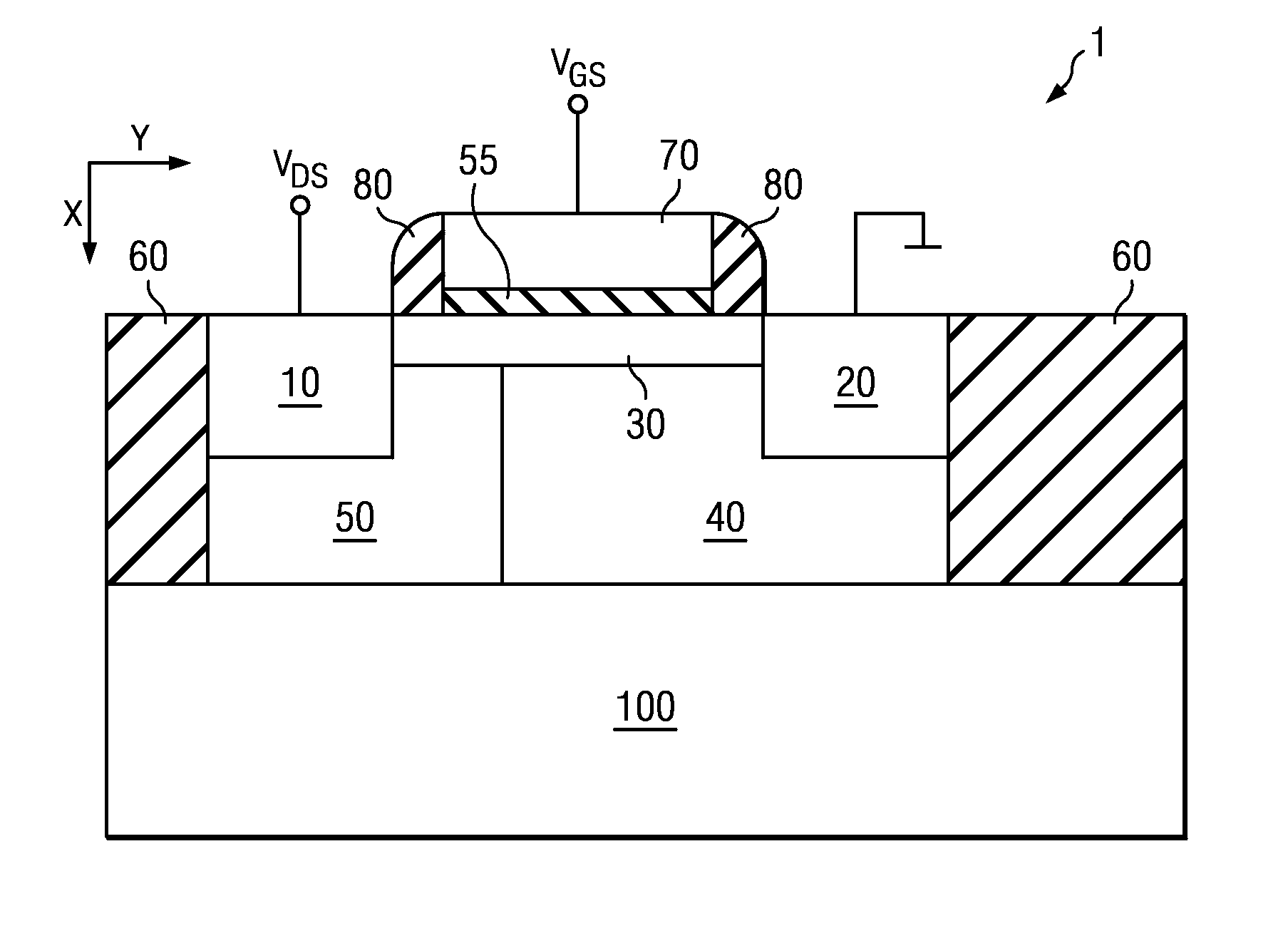
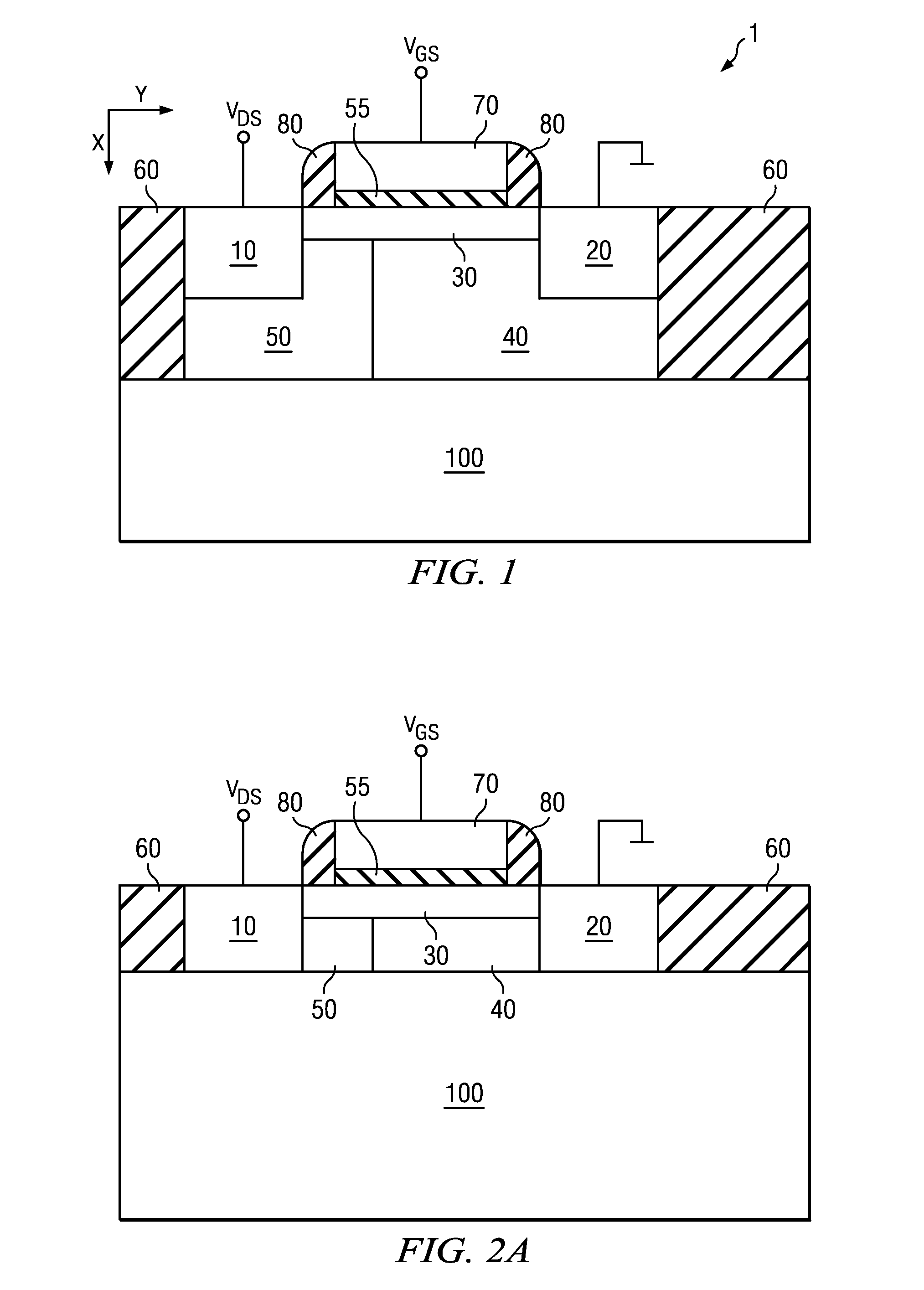
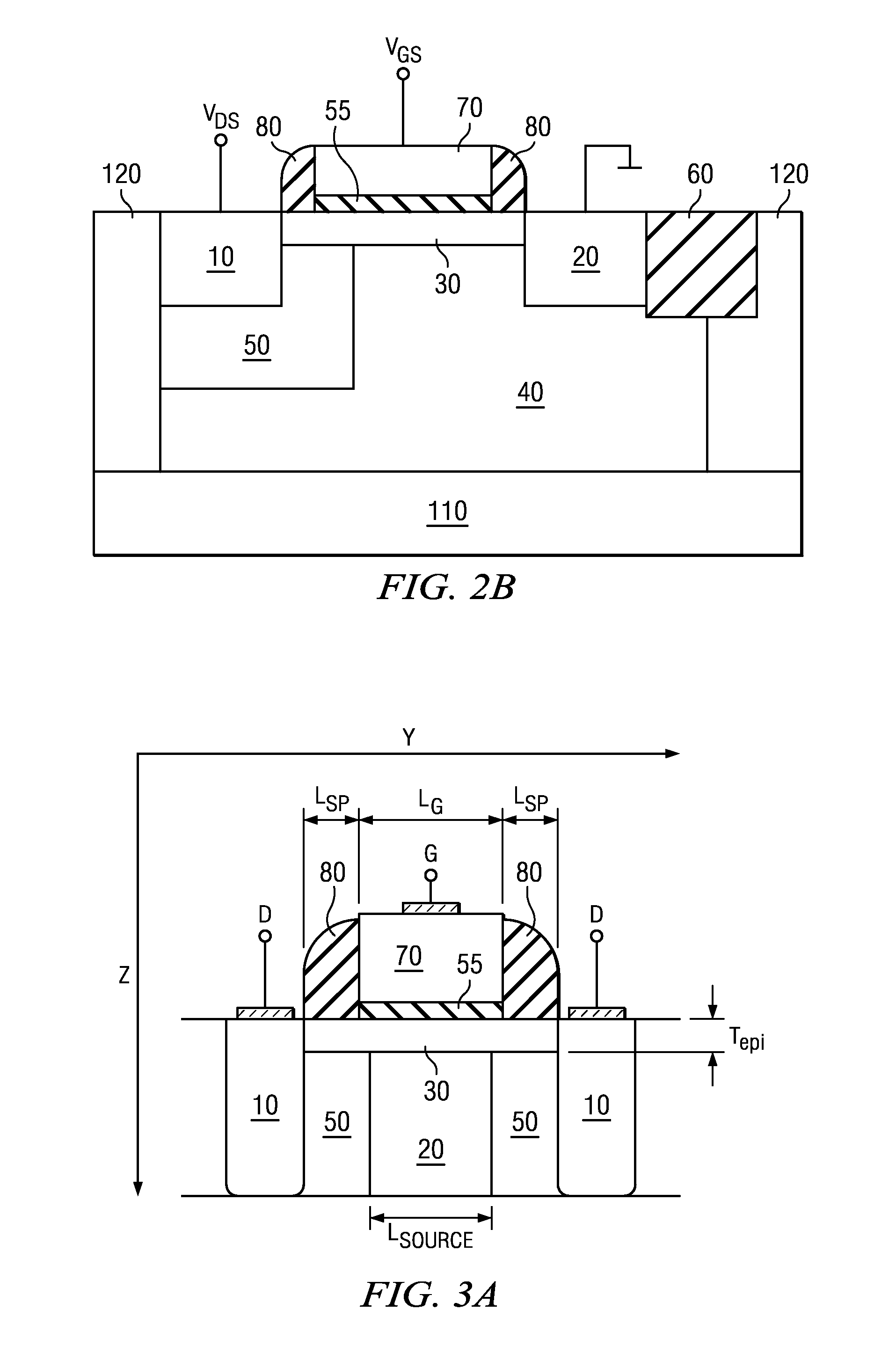
Tunnel field effect devices and methods of fabricating tunnel field effect devices are described. In one embodiment, the semiconductor device includes a first drain region of a first conductivity type disposed in a first region of a substrate, a first source region of a second conductivity type disposed in the substrate, the second conductivity type being opposite the first conductivity type, a first channel region electrically coupled between the first source region and the first drain region, the first source region underlying a least a portion of the first channel region, and a first gate stack overlying the first channel region.

Description

TECHNICAL FIELD[0001]The present invention relates generally to semiconductor devices and, in particular embodiments, to tunnel field effect transistors.BACKGROUND[0002]For almost four decades, the progress of microelectronics, as defined by Moore's Law, has been based on the constant optimization of cost-efficient materials, processes and technologies. For sub-100 nm technologies, conventional scaling has become challenging.[0003]Scaling without a loss of performance requires scaling down source / drain regions and gate oxide thickness to maintain sufficient gate control. However, in practice, the pace of scaling both gate oxide and source / drain junctions has reduced. Gate oxide scaling has slowed down due to increased gate leakage, while source / drain junction scaling has been hampered due to increased resistance due to inability to increase dopant solubility. As a practical matter, this manifests as an increase in short channel effects such as drain induced barrier lowering. The los...

Claims


Application Information

Patent Timeline
IPC IPC(8): H01L29/78H01L21/336
CPCH01L21/26506H01L21/26586H01L29/7391H01L29/165H01L29/66356H01L29/0692H01L21/2658H01L29/0895H01L29/88H01L29/66742H01L29/66977H01L29/78603H01L29/78621H01L29/78696
Inventor GOSSNER, HARALDRAO, RAMGOPALASRA, RAM
Owner INFINEON TECH AG
Learn More