
Display device and method of manufacturing the same

a technology of display device and barrier layer, which is applied in the field of display device, can solve the problems of constant rate of bonding failure, deterioration of productivity, increase in cost, etc., and achieve the effect of improving productivity

Active Publication Date: 2011-06-23
TRIVALE TECH LLC
View PDF8 Cites 20 Cited by
  • Summary
  • Abstract
  • Description
  • Claims
  • Application Information

AI Technical Summary

Benefits of technology

[0017]The present invention has been made to solve the above-mentioned problems, and an object of the present invention is to provide a display device capable of improving the productivity, and a method of manufacturing the same.
[0020]According to exemplary aspects of the present invention, it is possible to provide a display device capable of improving the productivity, and a method of manufacturing the same.

Problems solved by technology

In this method, however, a bonding failure inevitably occurs at a constant rate during the bonding process.
Accordingly, it is expected that the LCD, which is a component of high value, becomes defective, resulting in increase in cost.
Additionally, it is necessary to accurately align and bond the glass substrate with the parallax barrier for each LCD, resulting in deterioration in productivity.
This causes a problem of an increase in the number of steps.
On the other hand, when one of the parallax barrier pattern and the black matrix pattern is formed using a black resin, instead of forming the both patterns using the same metallic film, the use of the black resin makes it difficult to achieve thinning.
This causes a problem that it is difficult to apply such a method to a high-definition LCD.
Thus, the substrate strength is insufficient, which makes difficult to manufacture the LCD.
This may make it difficult to continuously perform the subsequent manufacturing steps.
Besides, a crack or a wrinkle may occur in the thick resin layer due to its shrinkage, resulting in deterioration of the display quality.
Thus, the method disclosed in Japanese Unexamined Patent Application Publication No. 2005-258016 has problems involving the thick resin layer.
Besides, since two sets of the parallax barrier layer, the adhesion layer, and the glass substrate are stacked, the productivity thereof is not high.

Method used


Image

  • Display device and method of manufacturing the same
  • Display device and method of manufacturing the same
  • Display device and method of manufacturing the same

Examples


first exemplary embodiment

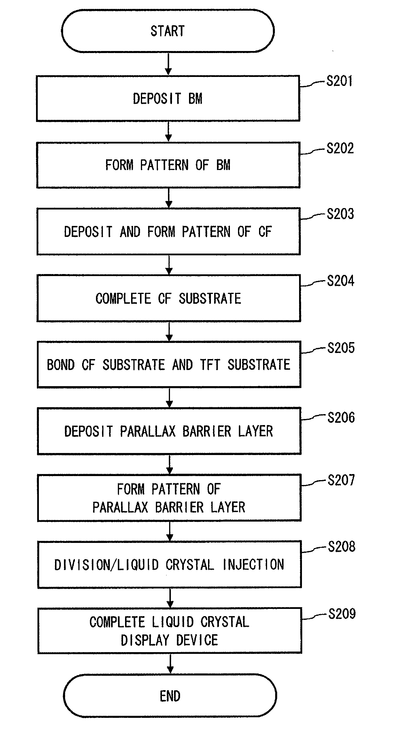
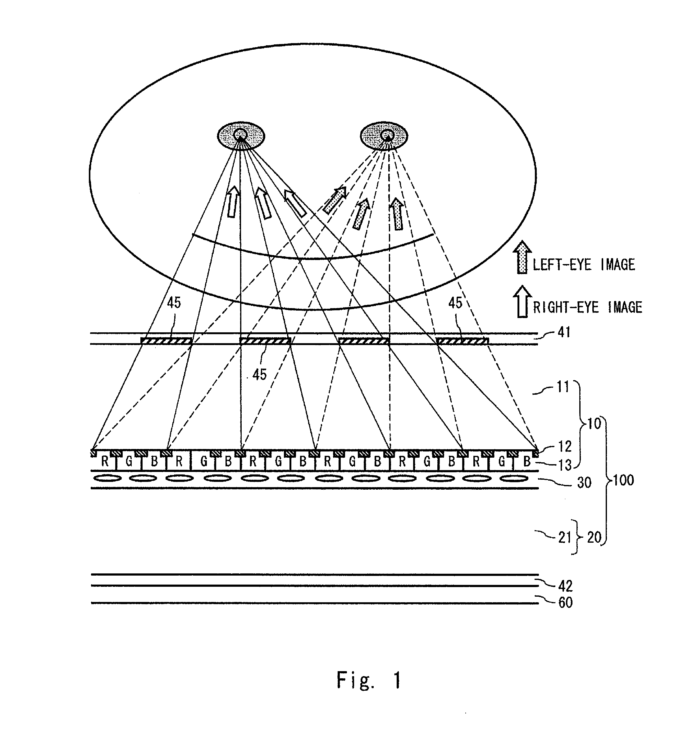
[0036]Referring first to FIG. 1, a display device according to a first exemplary embodiment of the present invention will be described. FIG. 1 is a sectional view showing a structure of a liquid crystal display device as an example of the display device according to the first exemplary embodiment. FIG. 1 shows a partial section within a display area. The display device according to the first exemplary embodiment is described by exemplifying an active-matrix type liquid crystal display device, but is illustrated by way of example only. Alternatively, a flat display device (flat panel display) such as an organic EL display device may also be employed.

[0037]The display device according to the first exemplary embodiment is a display device capable of displaying different images to different viewpoints, when the images are viewed from at least two viewpoints. The term “viewpoint” herein described refers to a position of each of the right and left eyes of a viewer, for example. If there a...

second exemplary embodiment

[0078]A display device according to a second exemplary embodiment of the present invention will be described with reference to FIG. 6. FIG. 6 is a sectional view showing a structure of a liquid crystal display device as an example of the display device according to the second exemplary embodiment. FIG. 6 shows a partial section within a display area. The second exemplary embodiment exemplifies a preferred embodiment in which the present invention is mainly applied to a dual-screen display device. Components similar to those of the liquid crystal display device of the first exemplary embodiment shown in FIG. 1 are denoted by the same reference numerals, and only differences will be described below.

[0079]Referring to FIG. 6, the thickness of the substrate on which the parallax barrier layer 45 is formed, i.e., the thickness of the substrate 11 of the CF substrate 10 according to the second exemplary embodiment is different from that of the first exemplary embodiment. The thickness the...

third exemplary embodiment

[0096]A display device according to a third exemplary embodiment of the present invention will be described with reference to FIGS. 11 and 12. FIG. 11 is a top view showing an overall structure of a liquid crystal display device as an example of the display device according to the third exemplary embodiment. FIG. 12 is a sectional view taken along the line XII-XII of FIG. 11. FIG. 13 is a perspective diagram to explain the relations of a holding member and a liquid crystal display panel. Components similar to those of the liquid crystal display device of the second exemplary embodiment shown in FIG. 6 are denoted by the same reference numerals, and only differences will be described below.

[0097]As described in the second exemplary embodiment, the panels which are cut out from the cell substrate 300 after the cell substrate 300 is thinned and the parallax barrier layer 45 is formed thereon have a thickness after thinning of about 0.1 mm or 0.3 mm. Thus, the panels are liable to be da...


PUM

PropertyMeasurementUnit
Thicknessaaaaaaaaaa
Distanceaaaaaaaaaa

Abstract

A method of manufacturing a display device according to one aspect of the present invention is a method of manufacturing a display device including a liquid crystal interposed between a CF substrate and a TFT substrate that are opposed to each other, the method including the steps of: bonding the CF substrate and the TFT substrate each having a mother substrate shape to form a cell substrate from which at least one panel is to be cut out; forming, after formation of the cell substrate, a parallax barrier layer for separating a display image on an outer side of the cell substrate at a side of one of the CF substrate and the TFT substrate; and dividing, after formation of the parallax barrier layer, the cell substrate into at least one panel.

Description

INCORPORATION BY REFERENCE[0001]This application is based upon and claims the benefit of priority from Japanese patent application No. 2009-289451, filed on Dec. 21, 2009, the disclosure of which is incorporated herein in its entirety by reference.BACKGROUND OF THE INVENTION[0002]1. Field of the Invention[0003]The present invention relates to a display device and a method of manufacturing the same, and more particularly, to a display device with a parallax barrier layer, and a method of manufacturing the same.[0004]2. Description of Related Art[0005]In recent years, liquid crystal display devices (LCDs) for displaying an image that varies depending on viewing angles are applied as 3D-LCDs and dual-screen LCDs. A 3D-LCD displays a 3D image using a parallax generated by allowing the viewer's right and left eyes to perceive images seen from different points. Thus, the 3D-LCD is also called a three-dimensional liquid crystal display device (e.g., Japanese Unexamined Patent Application P...

Claims


Application Information

Patent Timeline
IPC IPC(8): G02F1/1335B32B38/00G02B30/30
CPCB32B37/02B32B38/0004B32B2309/10B32B2457/202G02B27/2214Y10T156/1059G02B27/22G02F1/1333G02B27/225H04N13/0409H04N2013/0465H04N13/31H04N2013/405G02B30/30G02B30/27
Inventor NAKAYAMA, AKIO
Owner TRIVALE TECH LLC
Learn More