Method of manufacturing transferable elements incorporating radiation enabled lift off for allowing transfer from host substrate

a technology of transferable elements and lift off, which is applied in the manufacture of semiconductor/solid-state devices, electrical apparatus, semiconductor devices, etc., can solve the problems of decomposition and/or weakening of the interfacial layer or sacrificial layer, and achieve the effect of avoiding the use of silicon wafer as a host substra

Active Publication Date: 2011-06-23
EPISTAR CORP
View PDF70 Cites 238 Cited by
  • Summary
  • Abstract
  • Description
  • Claims
  • Application Information

AI Technical Summary

Benefits of technology

[0009]The present invention is directed to methods of manufacturing transferable elements, such as semiconductor die, that incorporates any one of several radiation enabled lift off techniques that allows the transfer of semiconductor die, from a host substrate with or without the need for anchoring structures and an intermediate substrate. Use of a silicon wafer as a host substrate is avoided. The host substrate is substantially optically transparent to selected radiation, for example of a laser, while the epitaxial material itself, or a sacrificial layer deposited at the interface between the host substrate and epitaxial layer, exhibits substantially absorptive properties. Application of laser radiation results in dec...

Problems solved by technology

Application of laser radiation results in decomposition and/or weakening of the interfacial layer or sa...

Method used


Image

  • Method of manufacturing transferable elements incorporating radiation enabled lift off for allowing transfer from host substrate
  • Method of manufacturing transferable elements incorporating radiation enabled lift off for allowing transfer from host substrate
  • Method of manufacturing transferable elements incorporating radiation enabled lift off for allowing transfer from host substrate

Examples


first exemplary embodiment

of Method

Single Step Radiation Lift Off to Stamp

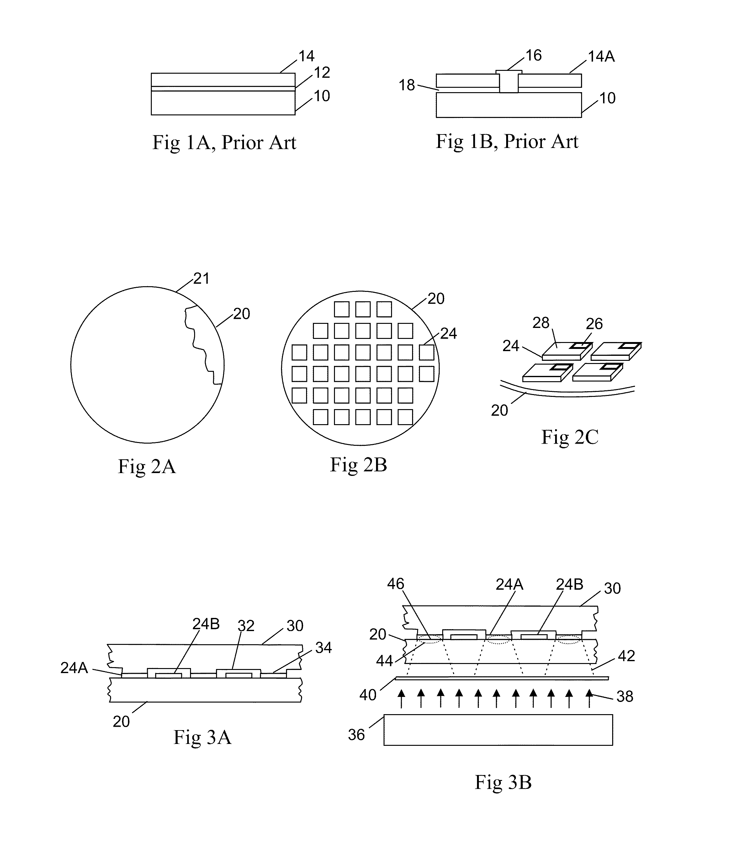
[0064]Referring to FIG. 2A, in the first exemplary embodiment of the manufacturing method a host substrate 20 is provided. The host substrate 20 is formed of a material, such as sapphire or the like, exhibiting substantial optical transparency to radiation, such as UV light, as described above. An epitaxial layer 21, which may include one or more layers, is grown on the host substrate 20 and processed and formed, for example, by using the well-known patterning and etching techniques, into semiconductor die 24 disposed on the host substrate 20 as shown in FIG. 2B. While square semiconductor die 24 have been shown, other shapes are possible, including rectangular, hexagonal, circular, polygonal, regular, irregular, compound or slotted. FIG. 2C depicts a partial view of the host substrate 20 with semiconductor die 24 that have each been metalized with n contact areas 26 and p contact areas 28. In one example the semiconductor die may have...

second exemplary embodiment

of Method

Two Step Laser Radiation Lift Off

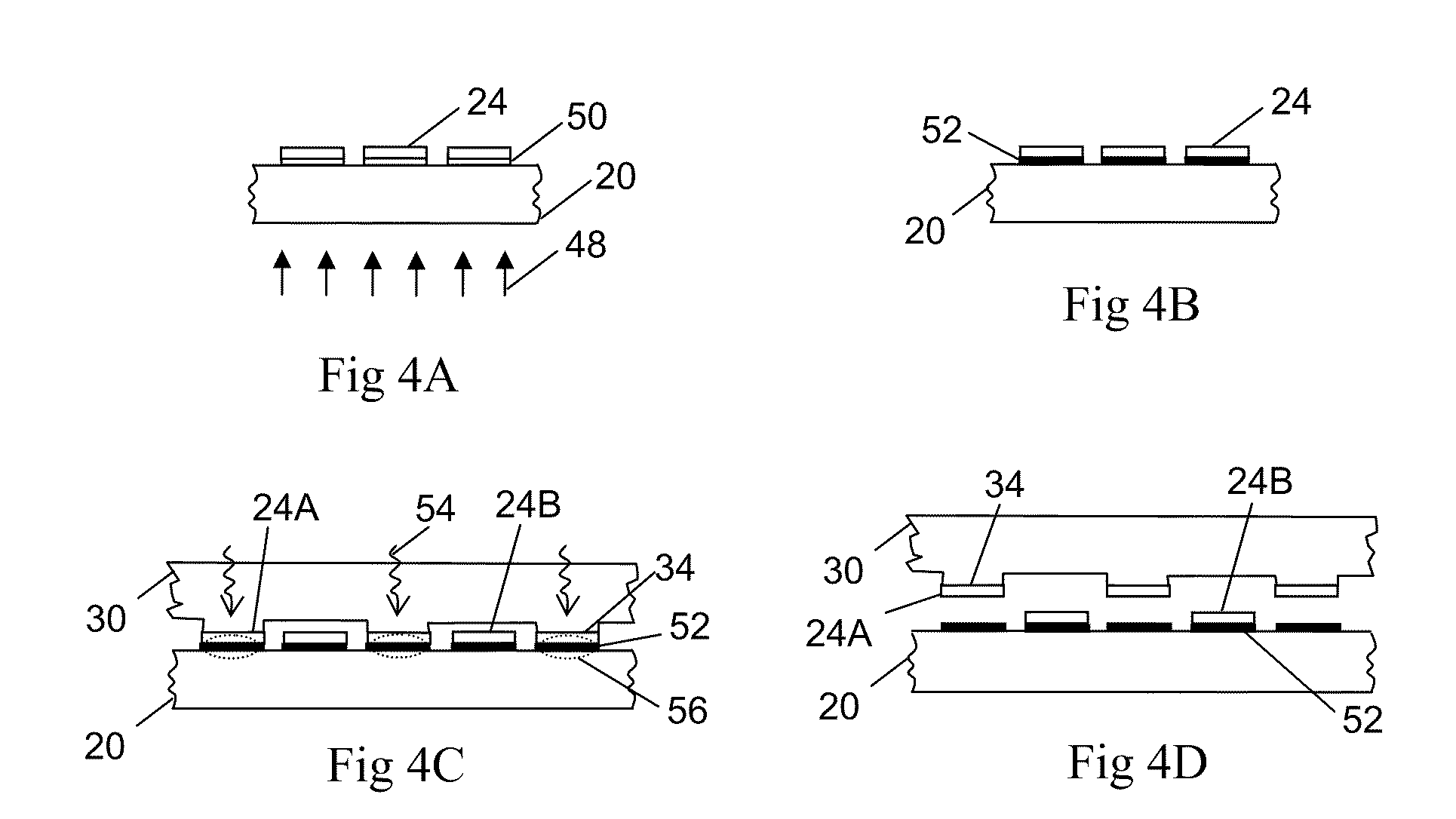
[0075]In a second exemplary embodiment of the manufacturing method it is possible to decompose the GaN layer during the irradiation step while not releasing the semiconductor die 24A from the host substrate 20. In this embodiment irradiation of the interface layer decomposes the GaN into N2 gas and metallic Ga. The metallic gallium present in the interface layer continues to bind the semiconductor die 24A to the host substrate 20. In a second step subsequent application of a temperature sufficient to melt the gallium layer will then allow for the release of the semiconductor die. Due to the relatively low melting point of gallium, this temperature could be in the region of 30° C.

[0076]FIGS. 4A-4D illustrate this two step laser lift off technique employed in the second exemplary embodiment of the method of the present invention. Initially, the host substrate 20, made of optically transparent material, such as sapphire, is prepared with an epi...

third exemplary embodiment

of Method

Maintaining Semiconductor Die Location

[0078]In a third exemplary embodiment of the manufacturing method of the present invention, which is a variation of the above-described two step process, the entire wafer may be heated to a sufficient temperature to allow for reflow of the gallium layer 52. The stamp 30 may be configured to pick up semiconductor die 24A, as described above; but in order to control the position of the semiconductor die, several solutions are described hereinafter, with reference to FIGS. 5A-5F.

[0079]In FIG. 5A, a variation is shown where an optical system is used with the laser such that every second semiconductor die 62 is irradiated. Even if only some of these semiconductor die 62 are to be transferred to a stamp, or other substrate, the ones that are not picked up are restrained in sideways movement by the adjacent semiconductor die 64 that are still on a layer of solid gallium. The width d of the trenches 66 between the semiconductor die 62, 64 can b...


PUM


Abstract

Semiconductor material is formed on a host substrate of a material exhibiting optical transparency with an intervening radiation lift off layer. A transfer device, intermediate substrate or target substrate is brought into adhesive contact with the semiconductor material and the radiation lift off layer is irradiated to weaken it, allowing the semiconductor material to be transferred off the host substrate. Electronic devices may be formed in the semiconductor layer while it is attached to the host substrate or the intermediate substrate.

Description

[0001]This patent application claims the benefit of U.S. provisional application Nos. 61 / 287,797 and 61 / 375,127, respectively filed Dec. 18, 2009 and Aug. 19, 2010. The disclosures of said provisional applications are hereby incorporated herein by reference thereto.TECHNICAL FIELD[0002]The subject matter of the present invention is directed generally to the manufacture of transferable elements and, more particularly, is concerned with a method of manufacturing transferable elements incorporating radiation enabled lift off for allowing transfer from a host substrate.BACKGROUND ART[0003]Illumination based on semiconductor light sources, such as light-emitting diodes (LEDs), offers an efficient and long-lived alternative to fluorescent, high-intensity discharge and traditional incandescent lamps. Many LED light sources employ high powered LEDs, which pose thermal management problems and other related problems. Another drawback with state of the art LED devices is a high initial cost.[0...

Claims


Application Information

Patent Timeline
IPC IPC(8): H01L33/00
CPCH01L21/268H01L33/0095H01L33/0079H01L33/0093H01L21/6836H01L21/6835H01L2221/68322H01L2221/68354H01L2221/68381
Inventor SPEIER, INGO
Owner EPISTAR CORP
Why Eureka
Try Eureka