Method of fabricating patterned CZT and CdTe devices

a technology of patterned czt and cdte, which is applied in the field of semiconductor devices, can solve the problems of reducing the ability not being met in conventional czt radiation detector technology, and limited performance of gamma-ray and x-ray segmented radiation detectors used in imaging applications

Active Publication Date: 2011-06-30
REDLEN TECH
View PDF50 Cites 15 Cited by
  • Summary
  • Abstract
  • Description
  • Claims
  • Application Information

AI Technical Summary

Problems solved by technology

Heretofore these criteria have not been met in conventional CZT radiation detector technology.
However, the performance of gamma-ray and x-ray segmented radiation detectors used in imaging applications and fabricated from CZT crystals is often limited because conventional fabrication processes do not provide the desired contact properties.
Interpixel leakage currents act as a source of noise that reduces the ability of these spectrometers to resolve spectrally the unique radiological emissions from a wide variety of radioactive isotopes—i.e., results in a lower energy resolution (ER).
The so-called interpixel resistance is a key limitation to performance and is typically much lower than overall device resistivity.
It be believed that commercial pixilated or segmented CZT devices have been fabricated by the in...

Method used


Image

  • Method of fabricating patterned CZT and CdTe devices
  • Method of fabricating patterned CZT and CdTe devices
  • Method of fabricating patterned CZT and CdTe devices

Examples


Embodiment Construction

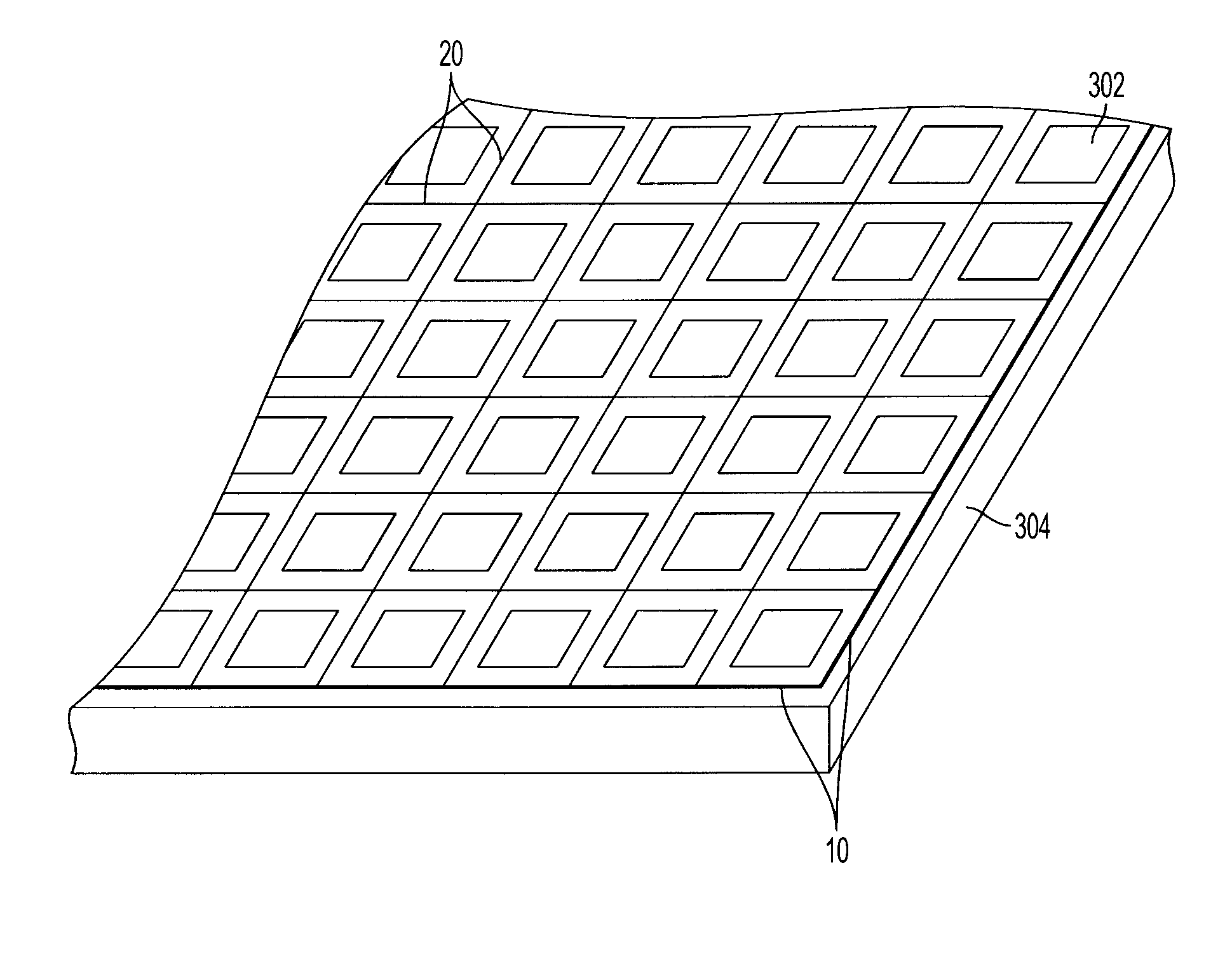
[0008]In one embodiment, a method of making a semiconductor radiation detector comprises providing a semiconductor substrate comprising front and rear major opposing surfaces, forming a solder mask layer over the rear major surface, and patterning the solder mask layer into a plurality of pixel separation regions. After the step of patterning the solder mask layer, the method further comprises forming anode pixels over the rear major surface. Additionally, in this embodiment, each anode pixel is formed between adjacent pixel-separation regions and a cathode electrode is located over the front major surface of the substrate.

[0009]In another embodiment, a radiation detector comprises a semiconductor substrate having opposing front and rear surfaces, a cathode electrode located over the front surface of said semiconductor substrate, a solder mask formed as a plurality of pixel separation regions and a plurality of anode pixels located over the rear surface of said semiconductor substra...


PUM


Abstract

A method of making a semiconductor radiation detector includes the steps of providing a semiconductor substrate having front and rear major opposing surfaces, forming a solder mask layer over the rear major surface, patterning the solder mask layer into a plurality of pixel separation regions, and after the step of patterning the solder mask layer, forming anode pixels over the rear major surface. Each anode pixel is formed between adjacent pixel-separation regions and a cathode electrode is located over the front major surface of the substrate. The solder mask can be used as a permanent photoresist in developing patterned electrodes on CdZnTe/CdTe devices as well as a permanent reliability protection coating. The method is very robust and ensures long-term reliability, outstanding detector performance, and may be used in applications such as medical imaging and for demanding other highly spectroscopic applications.

Description

BACKGROUND OF THE INVENTION[0001]The present invention relates generally to the field of semiconductor devices and particularly to radiation detectors.[0002]The general requirement for room temperature operation of a semiconducting material as a radiation detector and spectrometer (e.g., for a PET or CT scanner) is relatively large band gap energy such that thermal generation of charge carriers is kept to a minimum. Conversely, the requirement for high resolution is small band gap energy such that a large number of electron-hole pairs are created for an absorbed quantum of ionizing radiation. The material under consideration should also have a relatively high average atomic number if used in gamma ray spectroscopy to increase the gamma ray interaction probability. High charge carrier mobilities and long charge carrier lifetimes are also needed to ensure efficient charge carrier extraction and minimal effects from position-dependent charge collection. Detectors fabricated from Cadmiu...

Claims


Application Information

Patent Timeline
IPC IPC(8): H01L31/0224H01L31/18
CPCH01L31/02966Y02E10/547H01L31/1804H01L31/085
Inventor CHEN, HENRYMARTHANDAM, PRAMODHAAWADALLA, SALAHLU, PINGHE
Owner REDLEN TECH
Why Eureka
Try Eureka