Spr sensor

a sensor and sensor technology, applied in the field of sensors, can solve the problems of large size, further increase in size, and difficulty in achieving both miniaturization and multichannel detection of such a sensor, and achieve the effect of low cost and simple structur

Inactive Publication Date: 2011-06-30
NIIGATA UNIVERSITY +1
View PDF10 Cites 27 Cited by
  • Summary
  • Abstract
  • Description
  • Claims
  • Application Information

AI Technical Summary

Benefits of technology

[0039]According to the present invention, it is possible to provide an SPR sensor capable of achieving miniaturization and multichannel detection by a simple structure at a low cost.

Problems solved by technology

However, an SPR sensor having the above-described structure using a prism has a problem that its size is large, and even when such an SPR sensor is configured to achieve multichannel detection, its size is further increased.
For this reason, it is difficult for such an SPR sensor to achieve both miniaturization and multichannel detection.
However, such an optical waveguide-type SPR sensor requires two or more switching devices and therefore has a complicated structure, and in addition, it is difficult to produce such an optical waveguide-type SPR sensor at low cost.
However, each of these optical waveguide-type SPR sensors requires an array of two or more optical paths or a switching mechanism to achieve multichannel detection, which limits reduction in size.
Further, it is difficult to produce these optical waveguide-type SPR sensors at low cost.

Method used


Image

  • Spr sensor
  • Spr sensor
  • Spr sensor

Examples


example 1

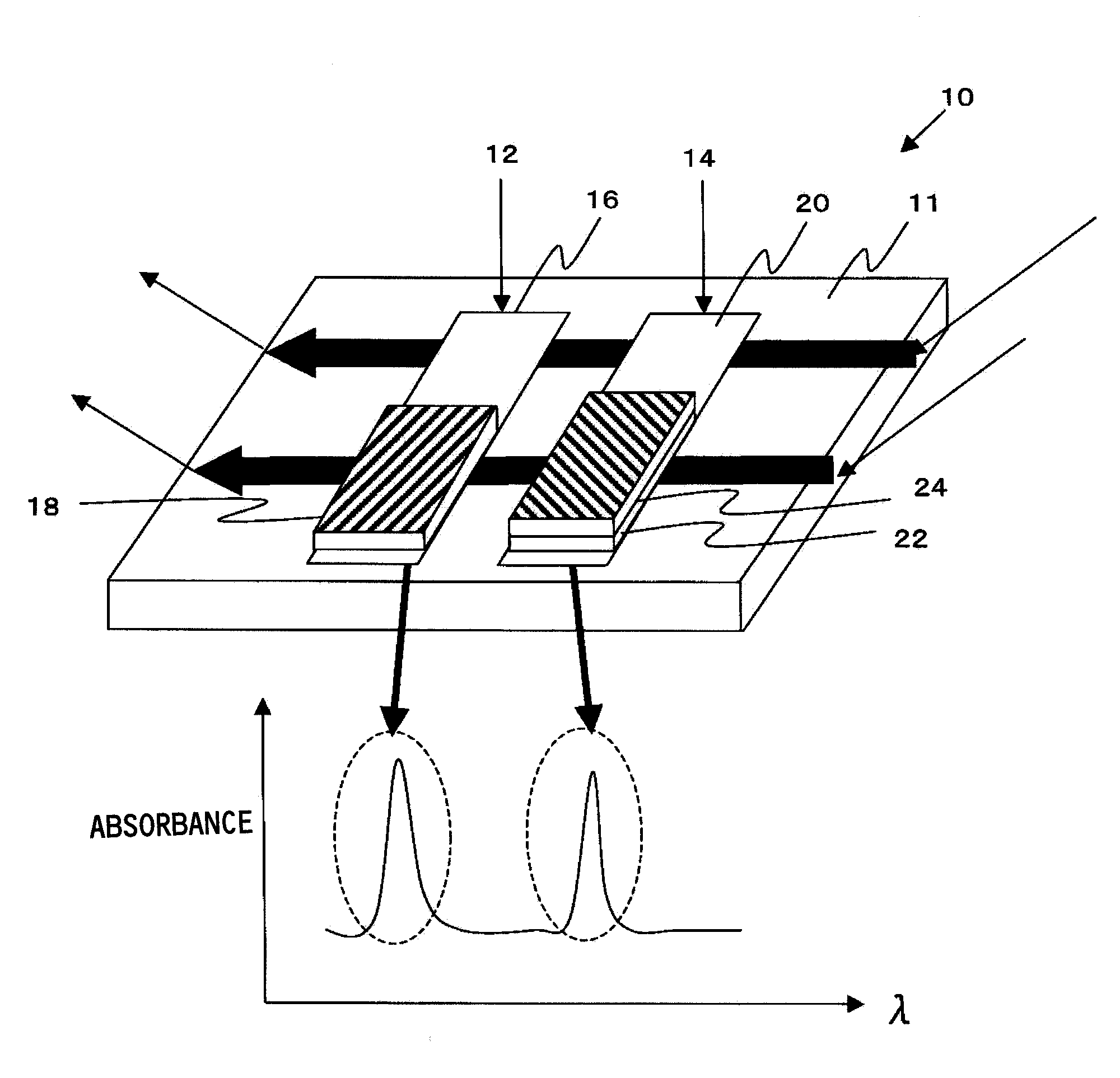
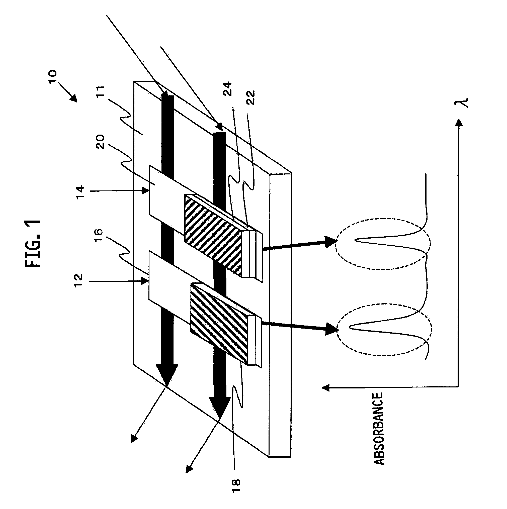
[0158]First, a slide glass (26 mm×26 mm) was prepared as a transparent substrate. Then, a 50-nm-thick layer made of Ag was formed as a metal layer on the slide glass by vacuum vapor deposition. At this time, the metal layers (7 mm×18 mm) were formed in two regions for use as detection regions by using a mask so that no metal layer was formed in a region other than the two regions. Then, as shown in FIG. 1, a 10 mg / mL PVK solution (solvent: toluene) was applied onto one-half of the surface of one of the two metal layers by a casting method to form a 20-nm-thick dielectric constant regulation layer (sensitive layer). On the other hand, a 100-nm-thick MgF2 layer was formed by vacuum vapor deposition on one-half of the surface of the other metal layer, and then a 20 mg / mL PVA solution (solvent: pure water) was applied onto the MgF2 layer by a casting method to form a 10-nm-thick sensitive layer so that a dielectric constant regulation layer composed of the MgF2 layer and the PVA layer w...

example 2

[0160]Metal layers were formed in two regions on a slide glass in the same manner as in Example 1. Then, a 20 mg / mL PVA solution (solvent: pure water) was applied onto one-half of the surface of one of the two metal layers by a casting method to form a 10-nm-thick dielectric constant regulation layer (sensitive layer). On the other hand, a 90-nm-thick MgF2 layer was formed by vacuum vapor deposition on one-half of the surface of the other metal layer, and then a 6 mg / mL PMMA solution (solvent: acetone) was applied onto the MgF2 layer by a casting method to form a 10-nm-thick PMMA layer (sensitive layer) so that a dielectric constant regulation layer composed of the MgF2 layer and the PMMA layer was formed.

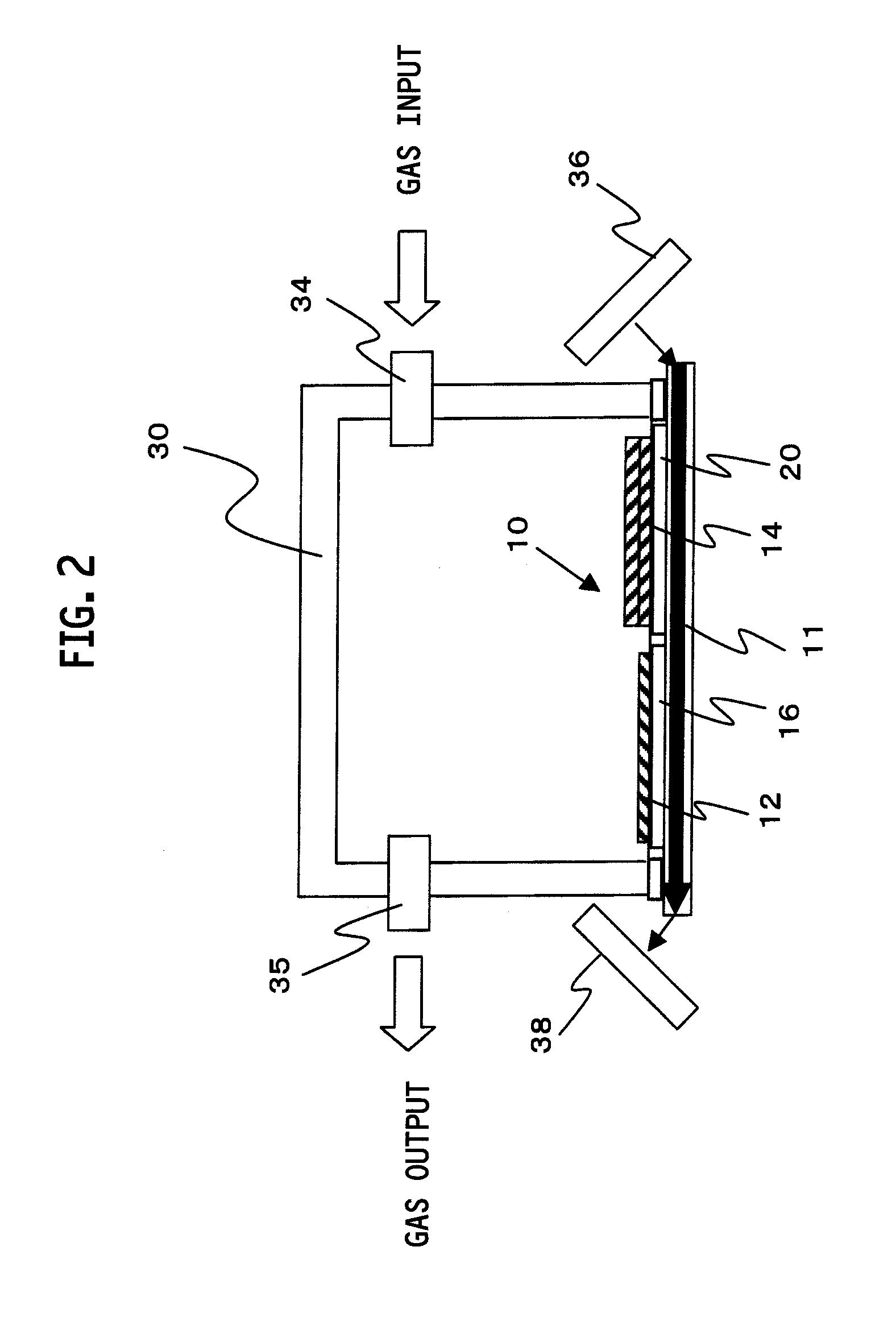
[0161]Then, a detection device such as one shown in FIG. 2 was produced in the same manner as in Example 1. Then, dry nitrogen passed through silica gel, wet nitrogen obtained by bubbling nitrogen in pure water, and toluene-nitrogen obtained by bubbling nitrogen in toluene were int...

example 3

[0162]Metal layers were formed in two regions on a slide glass in the same manner as in Example 1. Then, a mixture of a 5 mg / mL PVK solution and a 10 mg / mL octadecane solution (solvent: toluene) was applied onto one-half of the surface of one of the two metal layers by a dip coating method to form a 40-nm-thick dielectric constant regulation layer (sensitive layer). On the other hand, a 100-nm-thick MgF2 layer was formed by vacuum vapor deposition on one-half of the surface of the other metal layer, and then a 10 mg / mL PVA solution (solvent: pure water) was applied onto the MgF2 layer by a dip coating method to form a 55-nm-thick PVA layer (sensitive layer) so that a dielectric constant regulation layer composed of the MgF2 layer and the PVA layer was formed.

[0163]Then, a detection device such as one shown in FIG. 2 was produced in the same manner as in Example 1. Then, dry nitrogen passed through silica gel, wet nitrogen obtained by bubbling nitrogen in pure water, and toluene-nitr...


PUM

PropertyMeasurementUnit
thicknessaaaaaaaaaa
thicknessaaaaaaaaaa
dielectric constantaaaaaaaaaa

Abstract

Provided is an SPR sensor which can achieve compaction and multichannel detection by simple configuration at a low cost. The SPR sensor comprises an optical path, and detection areas on the side surface thereof formed by laminating metal layers formed to cause surface plasmon resonance phenomenon. The SPR sensor is characterized in that two or more detection areas are formed for one optical path, a dielectric constant regulation layer is further laminated in at least one of the two or more detection areas, dielectric constant is regulated to have a different surface plasmon resonance in each detection area, and a dielectric constant regulation layer laminated in the at least one of the two or more detection areas functions as a layer exhibiting sensitivity to an object to be detected.

Description

TECHNICAL FIELD[0001]The present invention relates to a sensor utilizing a surface plasmon resonance (SPR) phenomenon. More specifically, the present invention relates to an SPR sensor capable of simultaneously detecting two or more objects to be detected.BACKGROUND ART[0002]As a sensor capable of performing qualitative / quantitative analysis of an object to be detected with high sensitivity, an SPR sensor utilizing a surface plasmon resonance phenomenon has been proposed and practically used.[0003]As one example of a known structure of such an SPR sensor, there is a structure in which light emitted from a light source is allowed to enter the incidence plane of a high refractive index prism, which has a metal thin film on its plane different from the incident plane, at a predetermined incident angle so that the metal thin film being in contact with an object to be detected is irradiated with the light, and light produced by reflection at the boundary between the prism and the metal t...

Claims


Application Information

Patent Timeline
Patent Type & Authority Applications(United States)
IPC IPC(8): G01N21/55
CPCG01N21/553
Inventor MIYADERA, NOBUOMIZUSAWA, KENTASHINBO, KAZUNARIOHDAIRA, YASUOBABA, AKIRAKATO, KEIZOKANEKO, FUTAOKAWAKAMI, TAKAHIRO
Owner NIIGATA UNIVERSITY
Why Eureka
Try Eureka