Method for preparing organic light emitting diode and device thereof

Inactive Publication Date: 2011-06-30
NAT CHIAO TUNG UNIV
View PDF7 Cites 7 Cited by
  • Summary
  • Abstract
  • Description
  • Claims
  • Application Information

AI Technical Summary

Benefits of technology

[0018]To obtain the multilayer structure, a first organic molecule film is formed on the substrate first, and then a second organic molecule solution is applied to the first organic molecule film on the substrate so as to form a second organic molecule film. In so doing, interlayer miscibility is prevented.
[0019]To be specific, fabricating an organic light emitting diode with a multilayer structure according to the present invention essentially involves repeating the steps of dispensing the organic molecule solution, blade coating, and heating, in sequence. In so doing, it is feasible to form an organic light emitting diode with a multilayer structure. The method of the present invention is effective in effectuating the desirable number of layers of an organic light emitting diode and spreading the multilayer structure evenly using a whole-solution process, and is applicable to fabrication of a large-area photoelectric component.
[0026]With the method of the present invention, it is feasible to fabricate a patterned organic light emitting diode with a multilayer structure, and evenly spread the multilayer structure fabricated by a whole-solution fabrication process. Also, the method of the present invention is applicable to fabrication of a large-area photoelectric component and fit for patterning.

Problems solved by technology

However, the aforesaid evaporation technique incurs high costs and requires complicated operation and therefore is inapplicable to fabrication of large-area components or devices.
However, spin coating has a drawback, that is, during a process of fabricating a multilayer structure by spin coating, severe miscibility between the layers of the multilayer structure renders the fabrication process unstable and prevents the product from meeting industrial demand.
However, the aforesaid proposals are aimed at chemical materials and thus confronted with limitations, inflexibility, and narrow scope of application when applied to organic molecule structure design.
If patterned products are fabricated by a fabrication process that involves using inorganic light emitting diode, the light emitting diodes must be presented in the form of point light sources and arranged in an array, and in consequence the fabrication process will be intricate and will disadvantageously result in unevenness of light color.
The methods disclosed in the aforesaid literature are intricate, and the conditions for the fabrication process performed by the method are difficult to control, not to mention that the methods disadvantageously feature instability, low success rates of patterning, failure to fabricate patterns of any shapes, and low industrial applicability.

Method used


Image

  • Method for preparing organic light emitting diode and device thereof
  • Method for preparing organic light emitting diode and device thereof
  • Method for preparing organic light emitting diode and device thereof

Examples


Embodiment Construction

[0039]The present invention is herein illustrated with specific embodiments, so that one skilled in the pertinent art can easily understand other advantages and effects of the present invention from the disclosure of the invention.

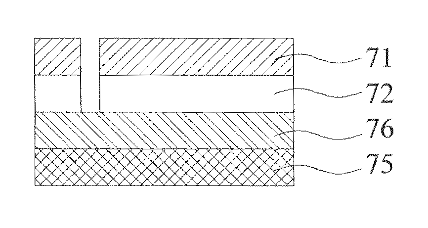
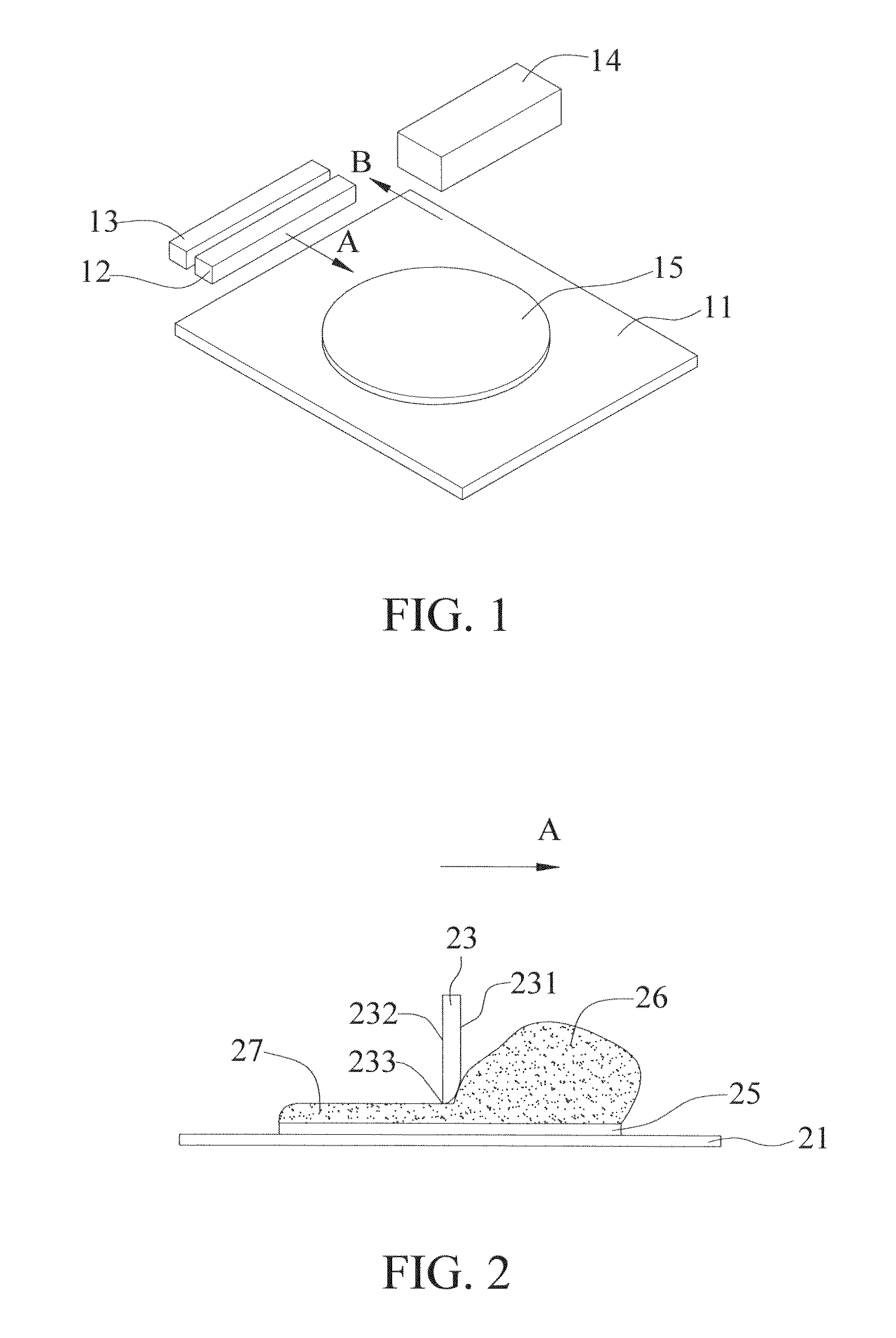
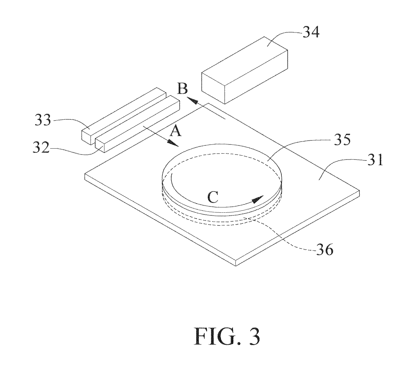
[0040]In general, an organic light emitting diode is fabricated by disposing on a glass substrate an anode formed by a layer of transparent conductive material made of, for example, tin-doped indium oxide (ITO), disposing on the anode a hole feeding layer, a hole conveying layer, an organic light emitting layer, an electron conveying layer, and an aluminum cathode in sequence, and applying a voltage to between the anode and the cathode, so as for the organic light emitting diode thus fabricated to emit light. The present invention provides a method for fabricating an organic light emitting diode. The method of the present invention attaches great importance to forming the multilayer structure of an organic molecule film, namely a hole feeding layer, a hole...


PUM


Abstract

A method for fabricating an organic light emitting diode and a device thereof are provided. The method includes: providing a substrate; dispensing to the substrate a second organic molecule solution resulting from dissolving a second organic molecule in a solvent; applying the second organic molecule solution to a surface of the substrate so as to form a wet film layer; and heating the wet film layer by a heating unit to remove the solvent therefrom and thereby form a second organic molecule film. The method is effective in fabricating a uniform multilayer structure for use in fabrication of large-area photoelectric components.

Description

BACKGROUND OF THE INVENTION[0001]1. Field of the Invention[0002]The present invention relates to a method and device for fabricating organic light emitting diodes, and more particularly, to a method and device for fabricating, by blade coating, an organic light emitting diode which has a multilayer structure and / or is patterned.[0003]2. Description of the Prior Art[0004]In general, an organic light emitting diode is fabricated by disposing on a glass substrate an anode formed by a layer of transparent conductive material made of, for example, tin-doped indium oxide (ITO), disposing on the anode a hole feeding layer, a hole conveying layer, an organic light emitting layer, an electron conveying layer, and an aluminum cathode in sequence, and applying a voltage to between the anode and the cathode, so as for the organic light emitting diode thus fabricated to emit light.[0005]Organic light emitting diodes are fabricated mostly by evaporation. For example, the fabrication process invol...

Claims


Application Information

Patent Timeline
IPC IPC(8): B05D5/06B05C9/14
CPCH01L27/3239H01L51/56H01L51/0003H10K59/221H10K71/12H10K71/441H10K71/166H10K71/00
Inventor HSU, CHAIN-SHUMENG, HSIN-FEIHORNG, SHENG-FUZAN, HSIAO-WENTSENG, HSIN-RONGYEH, CHUNG-LINGHSU, HUNG-WEILIU, CHANG-YAOYANG, HSIU-YUAN
Owner NAT CHIAO TUNG UNIV
Why Eureka
Try Eureka