Novel method for conformal plasma immersed ion implantation assisted by atomic layer deposition

a conformal plasma and ion implantation technology, applied in chemical vapor deposition coating, coating, metallic material coating process, etc., can solve the problems of increasing aspect ratio and shrinking device, reducing so as to achieve the effect of maximizing the penetration rate of dopant ions

Active Publication Date: 2011-06-30
APPLIED MATERIALS INC
View PDF29 Cites 405 Cited by
  • Summary
  • Abstract
  • Description
  • Claims
  • Application Information

AI Technical Summary

Problems solved by technology

Increasing aspect ratios and shrinking devices pose challenges to dopant implantation processes.
High energy implantation may drive ions to the bottom of the trench, but generally will not achieve conformal implantation and may result in over-implantation in the bottom of the trench and in field areas as compared to side walls.
However, any such benefit is minimal, particularly for very high aspect ratio structures, because electric field lines driving the motion of ions are orthogonal to the surface.

Method used


Image

  • Novel method for conformal plasma immersed ion implantation assisted by atomic layer deposition
  • Novel method for conformal plasma immersed ion implantation assisted by atomic layer deposition
  • Novel method for conformal plasma immersed ion implantation assisted by atomic layer deposition

Examples


Embodiment Construction

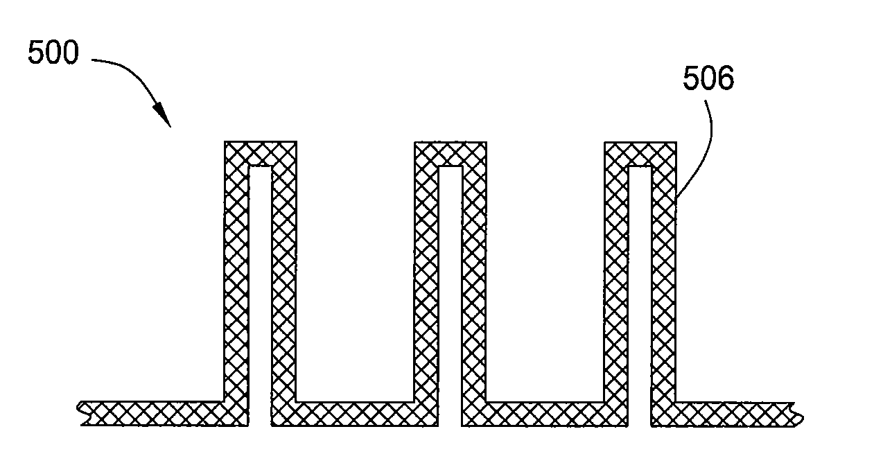
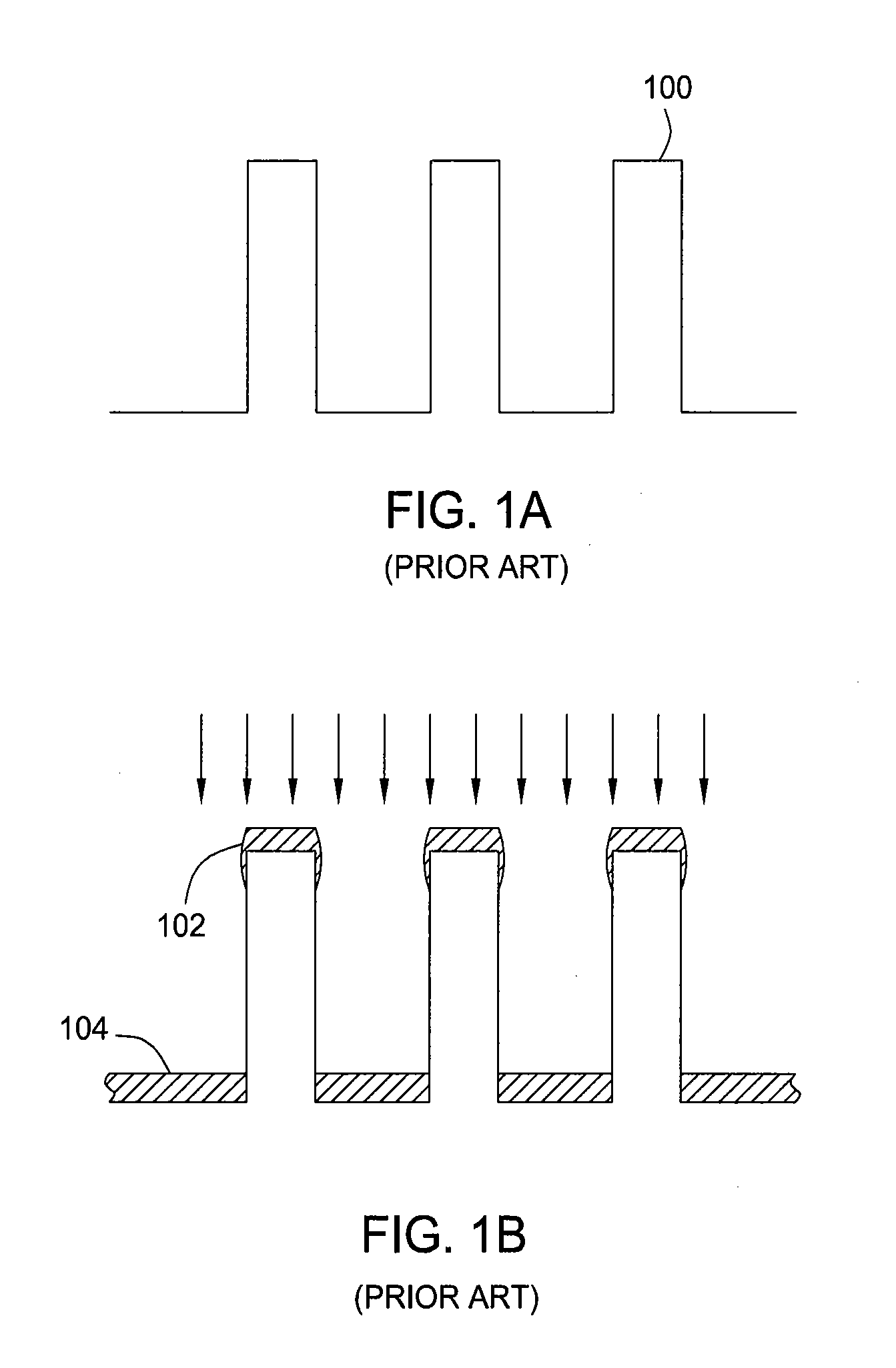
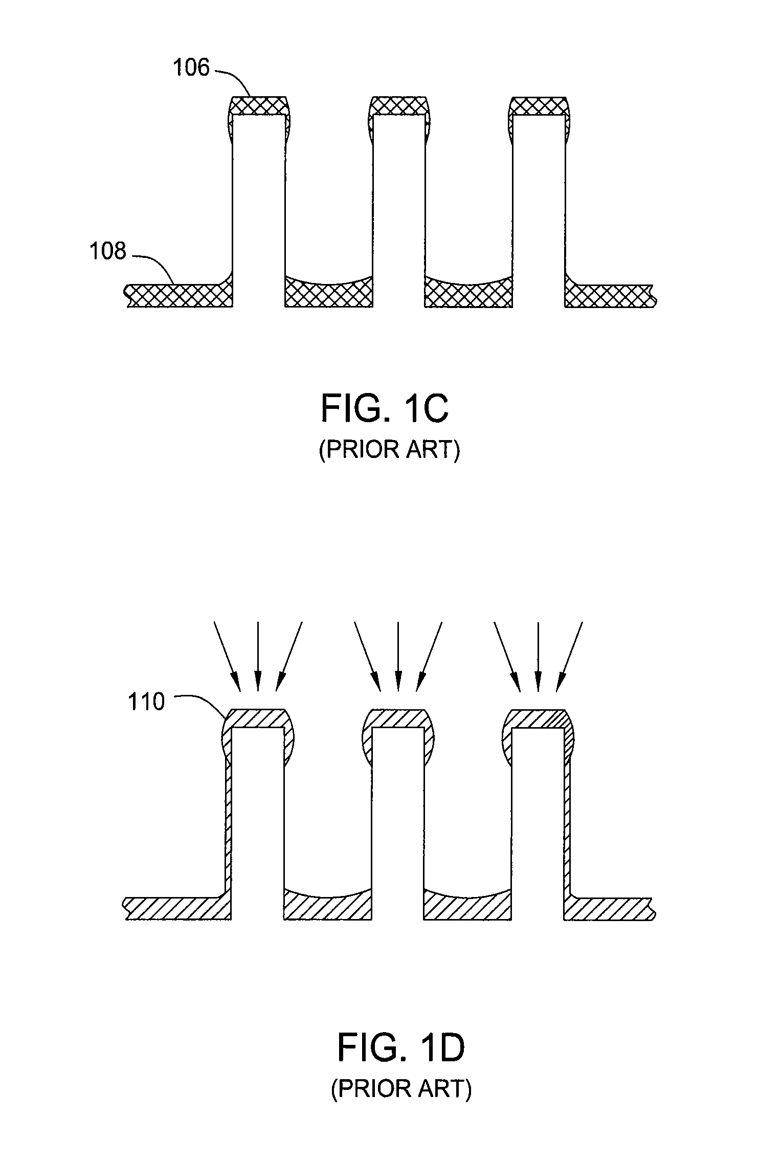
[0024]Embodiments of the invention contemplate methods of conformal doping of a substrate. Such methods generally provide for conformal deposition of a dopant source on a substrate followed by treatment with electromagnetic energy to diffuse the dopants into the substrate and activate them. Deposition may be by any process designed to achieve conformal deposition of thin dopant source layers on a substrate having high aspect ratio features, such as greater than about 3:1 by atomic layer deposition (ALD), chemical vapor deposition enhanced by weak plasma (WPCVD), or plasma-assisted atomic layer deposition (PAALD) of dopants on the substrate followed by anneal. Processes for manufacturing semiconductor devices are increasingly challenged to produce conformally doped regions on substrates with ultra-high aspect ratio holes or trenches formed in field regions. ALD is a successful procedure for forming conformal layers on high aspect ratio features heretofore used in metal and dielectric...


PUM

PropertyMeasurementUnit
temperatureaaaaaaaaaa
poweraaaaaaaaaa

Abstract

Embodiments of the invention provide a novel apparatus and methods for forming a conformal doped layer on the surface of a substrate. A substrate is provided to a process chamber, and a layer of dopant source material is deposited by plasma deposition, atomic layer deposition, or plasma-assisted atomic layer deposition. The substrate is then subjected to thermal processing to activate and diffuse dopants into the substrate surface.

Description

CROSS-REFERENCE TO RELATED APPLICATIONS[0001]This application is a divisional of co-pending U.S. patent application Ser. No. 12 / 028,423, filed Feb. 8, 2008, which is herein incorporated by reference.BACKGROUND OF THE INVENTION[0002]1. Field of the Invention[0003]Embodiments of the present invention generally relate to the fabrication of semiconductor devices and particularly to the formation of doped regions on a substrate by use of plasma implantation assisted by atomic layer deposition.[0004]2. Description of the Related Art[0005]In the semiconductor fabrication process, it is often necessary to impart impurities into a pure material. Called “doping,” this process invests the material with desirable properties, such as enhanced electrical conductivity. In many processes, it is advantageous to implant various atoms or ions into a semiconductor or semiconductor derivative substrate. For example, boron, phosphorus, and arsenic atoms or ions are routinely implanted into silicon substr...

Claims


Application Information

Patent Timeline
Patent Type & Authority Applications(United States)
IPC IPC(8): H01L21/22
CPCC23C16/45536H01L21/2236C23C16/56C23C16/505H01L21/265H01L21/0262
Inventor HANAWA, HIROJICHO, SEON-MEEFOAD, MAJEED A.
Owner APPLIED MATERIALS INC
Why Eureka
Try Eureka