Method of manufacturing CMOS image sensor using double hard mask layer

a technology of cmos image sensor and mask layer, which is applied in the direction of radio frequency controlled devices, instruments, television systems, etc., can solve the problems of difficult control of critical dimensions and complicated processes, and achieve the effect of easy control, thin thickness and critical dimensions

Inactive Publication Date: 2011-07-07
INTELLECTUAL VENTURES II
View PDF12 Cites 1 Cited by
  • Summary
  • Abstract
  • Description
  • Claims
  • Application Information

AI Technical Summary

Benefits of technology

[0021]According to the present invention, a thickness of the hard mask layer in the pixel region, into which the ions are implanted to form the photodiode, is different from a thickness of the hard mask layer in the logic region, into which the ions are not implanted, so that the process for removing the hard mask layer is not necessary. In addition, the hard mask layer has a thin thickness, so the critical dimension can be easily controlled when the gate pattern is formed. Further, since the organic anti-reflective layer is used as the anti-reflective layer, the uniformity of the critical dimension of the photoresist pattern can be improved.
[0022]In addition, since the reverse mask is not required, the hard mask layer may not remain in the gate pattern, so that various patterns can be utilized.
[0023]Further, the mask can be manufactured at a low cost as compared with the cost for the reverse mask, and the process for removing the hard mask layer can be omitted, so that the manufacturing cost and manufacturing time for the semiconductor device can be reduced.
[0024]In addition, according to the present invention, the thickness of the hard mask layer is reduced, the organic anti-reflective layer is used as the anti-reflective layer, and the process for removing the hard mask layer is omitted, so that the critical dimension of the gate pattern can be stably maintained, thereby improving the reliability and product yield of the semiconductor devices.

Problems solved by technology

However, according to the related art, the hard mask layer 14 is too thick, so the critical dimension may not be easily controlled when the gate pattern 13A is formed.
In addition, according to the related art, the residual hard mask layer must be removed to form the silicide, so the process may be complicated.

Method used


Image

  • Method of manufacturing CMOS image sensor using double hard mask layer
  • Method of manufacturing CMOS image sensor using double hard mask layer
  • Method of manufacturing CMOS image sensor using double hard mask layer

Examples


Embodiment Construction

Technical Problem

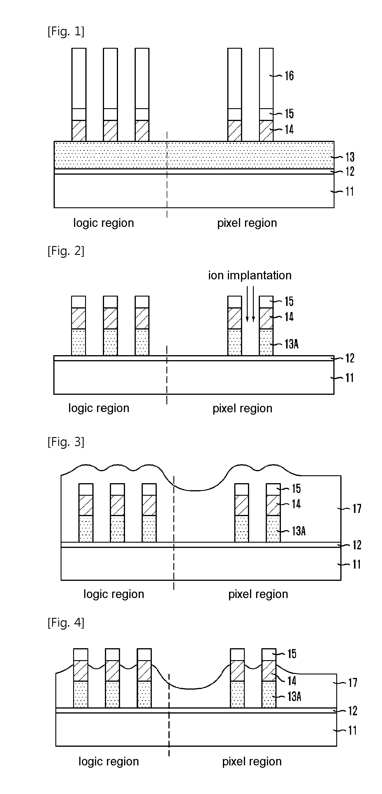
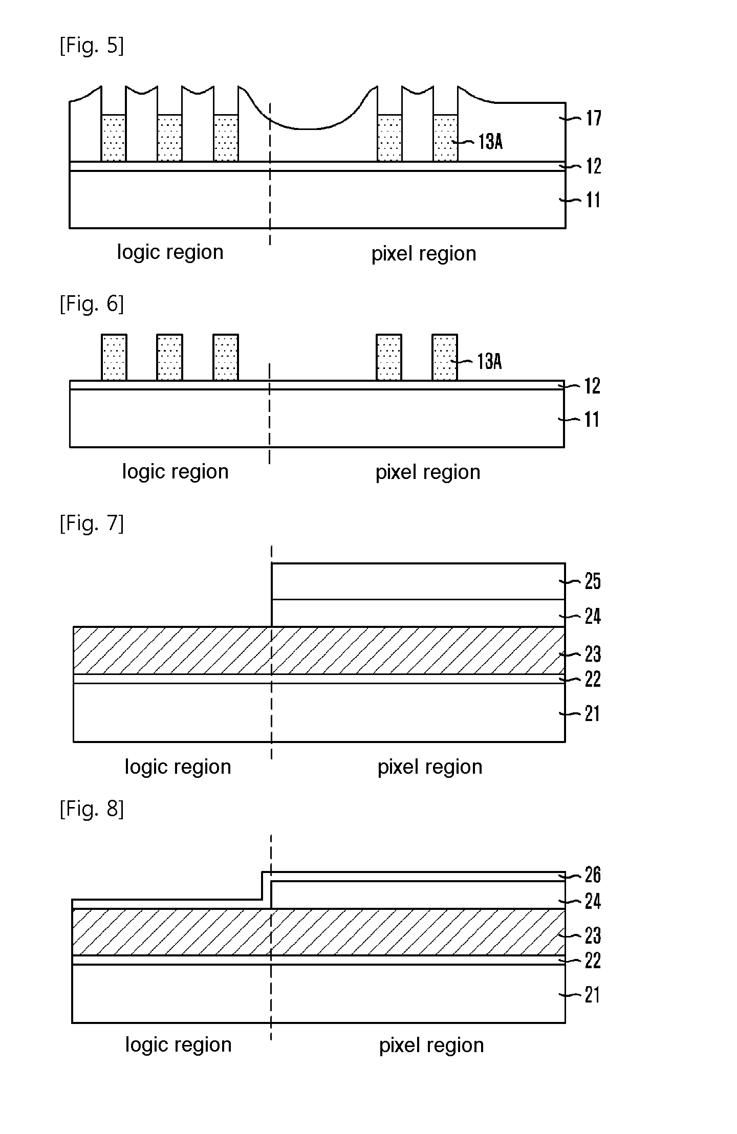
[0017]Accordingly, the present invention has been made to solve the above-mentioned problems occurring in the prior art, and the present invention provides a method of manufacturing a CMOS image sensor, capable of forming silicide in a logic region and facilitating ion implantation into a pixel region while keeping a hard mask layer at a thin thickness without performing a process for removing the hard mask layer.

Technical Solution

[0018]In addition, the present invention provides a method of manufacturing a CMOS image sensor, capable of easily controlling the critical dimension when forming a gate pattern while improving the uniformity of the critical dimension of a gate photoresist pattern.

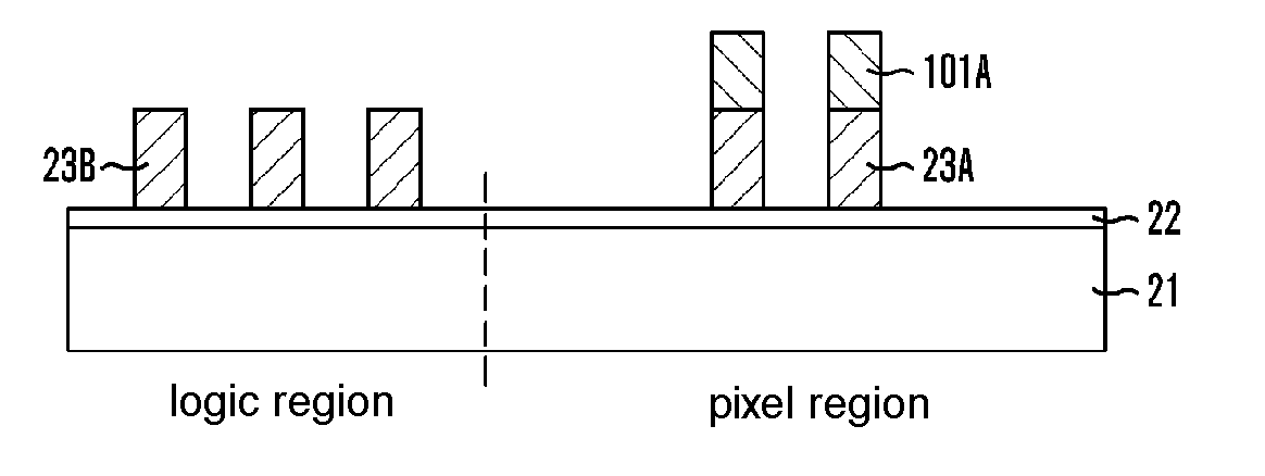
[0019]In accordance with an aspect of the present invention, there is provided a method of manufacturing a CMOS image sensor, the method including the steps of: forming a gate conductive layer on a substrate on which a pixel region and a logic region are defined; forming a hard m...


PUM

PropertyMeasurementUnit
gate conductiveaaaaaaaaaa
conductiveaaaaaaaaaa
insulatingaaaaaaaaaa

Abstract

Disclosed is a method of manufacturing a CMOS image sensor, capable of forming silicide in a logic region and facilitating ion implantation into a pixel region while keeping a hard mask layer in a thin thickness without performing a process for removing the hard mask layer. The critical dimension is easily controlled when forming a gate pattern and the uniformity in the critical dimension of a gate photoresist pattern is improved. The method includes the steps of forming a gate conductive layer on a substrate on which a pixel region and a logic region are defined; forming a hard mask pattern on the gate conductive layer in such a manner that a thickness of the hard mask pattern in the pixel region is thicker than a thickness of the hard mask pattern in the logic region; forming a gate pattern in the pixel region and the logic region by etching the gate conductive layer using the hard mask pattern as an etching barrier; removing the hard mask pattern remaining in the logic region; and forming silicide in the logic region.

Description

TECHNICAL FIELD[0001]The present invention relates to a method of manufacturing a semiconductor device. More particularly, the present invention relates to a method of manufacturing a CMOS image sensor using a double hard mask layer.BACKGROUND ART[0002]Among semiconductor devices, a CMOS image sensor is manufactured through a CMOS process and a unit pixel of the CMOS sensor includes one photodiode and three or four transistors for driving the unit pixel. Similar to transistors of general memory devices, the transistors of the CMOS image sensor may include a gate electrode and source / drain regions.[0003]When the ion implantation process is performed to form the photodiode of the CMOS image sensor, a thick hard mask is formed on an entire surface of a substrate as an ion implantation blocking material, and an inorganic anti-reflective layer including silicon oxynitride (SiON) is formed over the thick hard mask as an anti-reflective layer.[0004]FIGS. 1 to 6 are sectional views showing ...

Claims


Application Information

Patent Timeline
Patent Type & Authority Applications(United States)
IPC IPC(8): H04N5/335G03F7/20
CPCH01L27/14609H01L27/14689H01L27/14685H01L27/1462H01L27/146
Inventor BACK, WOON-SUCK
Owner INTELLECTUAL VENTURES II
Why Eureka
Try Eureka