Organic el device and method for manufacturing the same

Active Publication Date: 2011-07-21
SHARP KK
View PDF3 Cites 6 Cited by
  • Summary
  • Abstract
  • Description
  • Claims
  • Application Information

AI Technical Summary

Benefits of technology

[0016]Among the circumstances of recent years, in which development of organic EL displays with higher light emission efficiencies has been sought, this invention can provide an organic EL device which can maintain an excellent light emission efficiency over long periods. Moreover, because a protective layer of this invention has high visible-light transmittance, a configuration of this invention is particularly useful in top-emission type organic EL devices.

Problems solved by technology

Important problems for the commercialization of organic EL devices as color displays include, in addition to the realization of high definition, device long-term stability, including color reproducibility.
However, multicolor light-emitting organic EL devices have the drawback of a prominent decline in light emission characteristics (current-luminance characteristics) due to driving over a certain period.
Hence film fabrication methods developed for organic EL devices using semiconductor processes cannot be applied, and there has been the problem that a sealing thin film having adequate moisture-proof properties cannot be formed.
However, the sealing film in Patent Document 1 comprises a substantial quantity of silicon-silicon bonds, and so has low transmittance of visible light, and cannot be used as the sealing film in a top-emission structure.

Method used


Image

  • Organic el device and method for manufacturing the same
  • Organic el device and method for manufacturing the same
  • Organic el device and method for manufacturing the same

Examples


embodiments

Manufacturing Example 1

[0073]In this manufacturing example, by applying high-frequency power to a gas mixture of monosilane (SiH4), ammonia (NH3), and nitrogen, SiN:H film was formed, and the film characteristics were evaluated. In this manufacturing example, the monosilane flow rate was 100 sccm, the nitrogen flow rate was 2000 sccm, and the ammonia flow rate was varied in the range 20 to 110 sccm. At this time, the pressure of the gas mixture was 100 Pa. Using high-frequency power at a frequency of 27.12 MHz and power density of 0.5 W / cm2, SiN:H film was formed on a film substrate at 50° C.

(1) Si, N, and H Content—

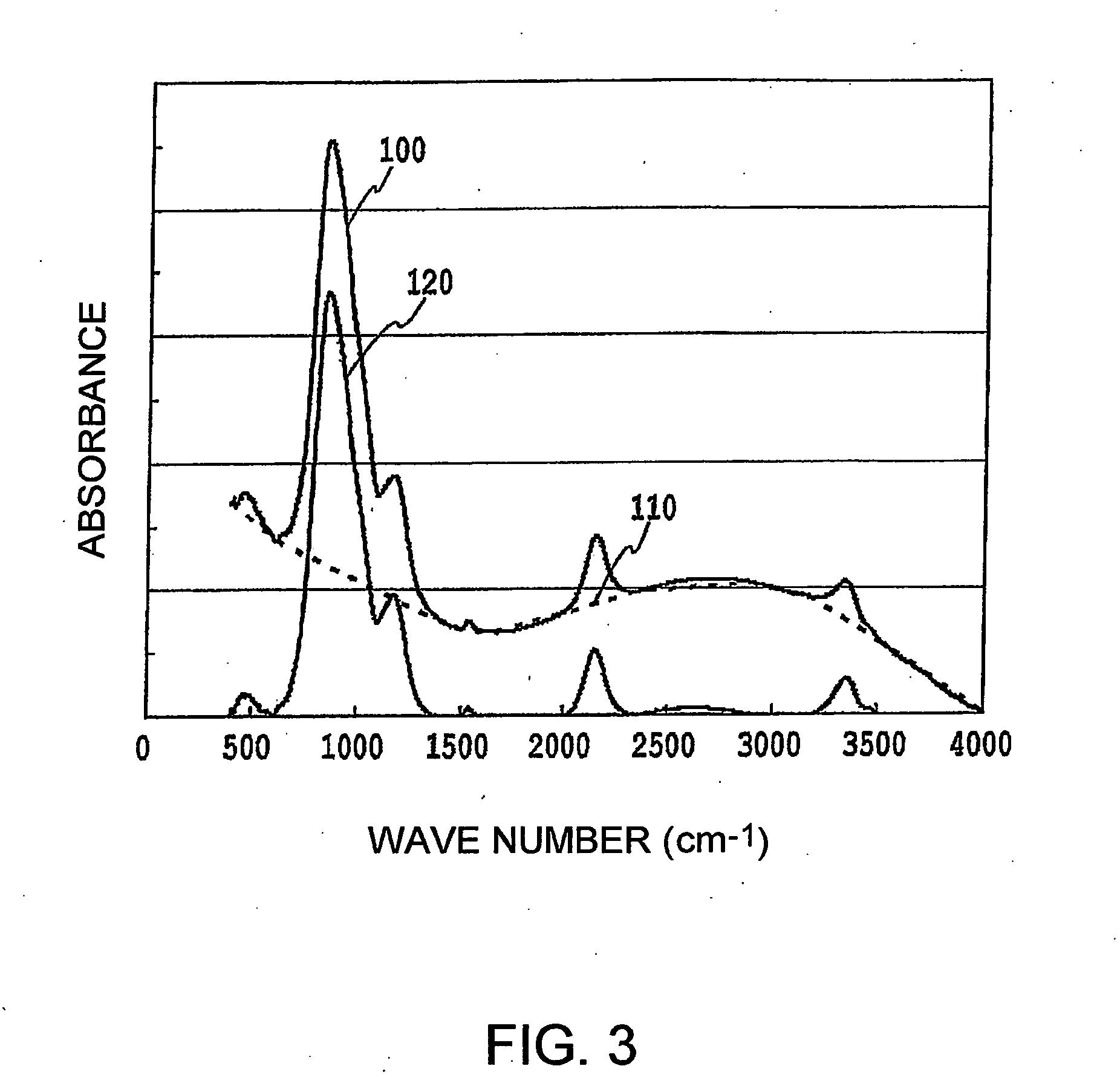
[0074]As the film substrate, a Si wafer of thickness 0.5 mm was used, and SiN:H film of thickness 1 μm was formed. An elastic recoil particle detection method and Rutherford backscattering method were combined in analyses of the SiN:H film obtained, and the contents of Si, N, and H in the SiN:H film were determined. The results appear in Table 1.

(2) N—H / Si—N Area Ratio a...

manufacturing example 2

[0083]In this manufacturing example, the ammonia flow rate was fixed at 80 sccm, and the frequency of the high-frequency power applied was changed to 40.68 MHz or 13.56 MHz; otherwise, the same procedure used in Manufacturing Example 1 was used to form SiN:H film on film substrates. Evaluations similar to those of Manufacturing Example 1 were performed for the SiN:H films obtained. Results appear in Table 2.

TABLE 2Effect of frequency of high-frequency powerCompositionSi—H / Si—NN—H / Si—NUnmodifiedExtinctionFilmSampleFrequency(at %)areaareaportion areacoefficientstressnumber(MHz)SiNHratioratioratio (%)(×10−4)(MPa)727.1232.437.730.00.1630.091952111140.6831.737.529.90.1580.086961.8161213.5627.439.333.30.1930.125252.18SiH4 flow rate: 100 sccm, NH3 flow rate: 80 sccm

[0084]From Table 2, it is clear that similarly to sample 7 fabricated using high-frequency power at 27.12 MHz, excellent characteristics are exhibited by sample 11, fabricated using high-frequency power at 40.68 MHz. On the othe...
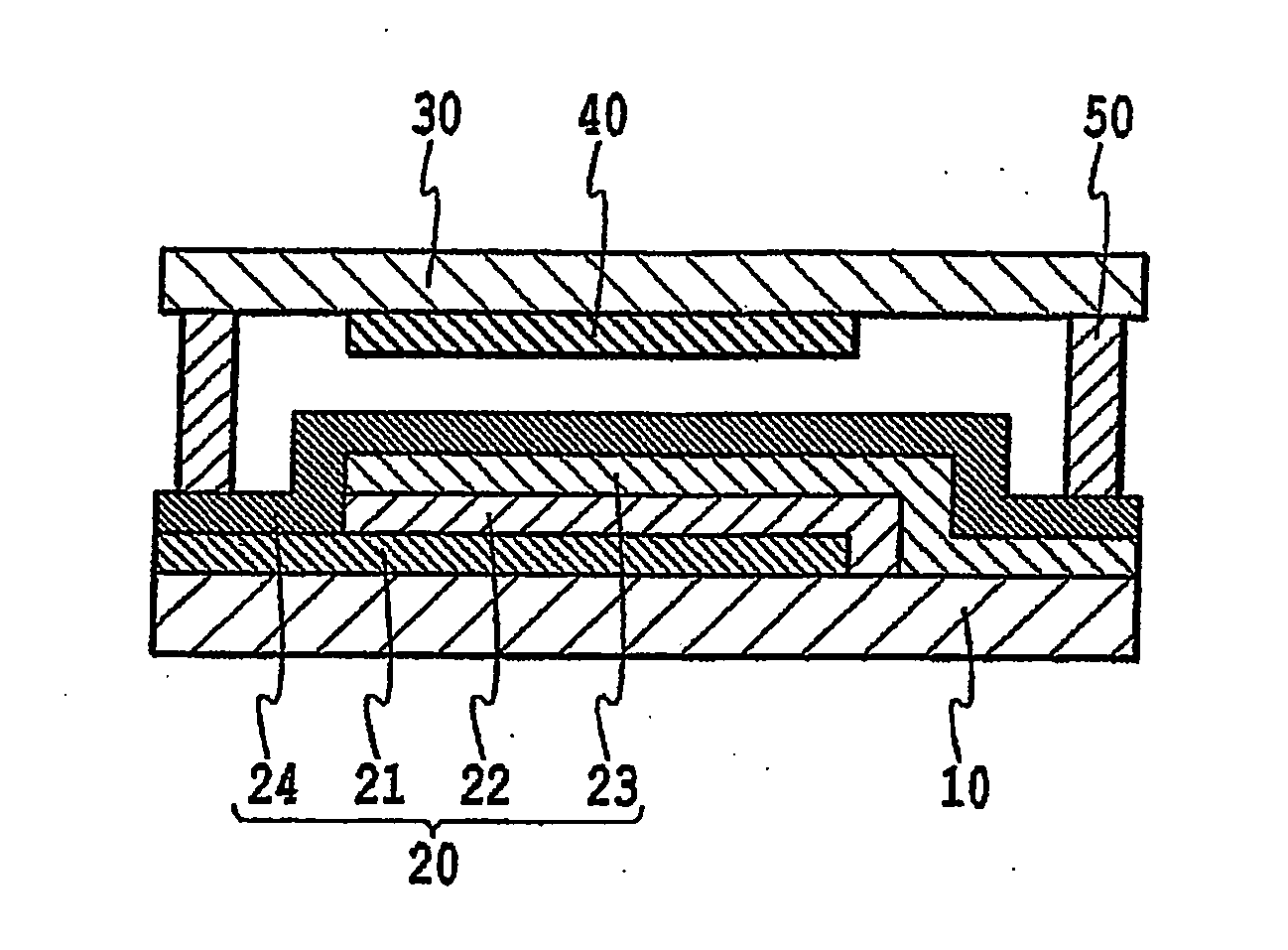
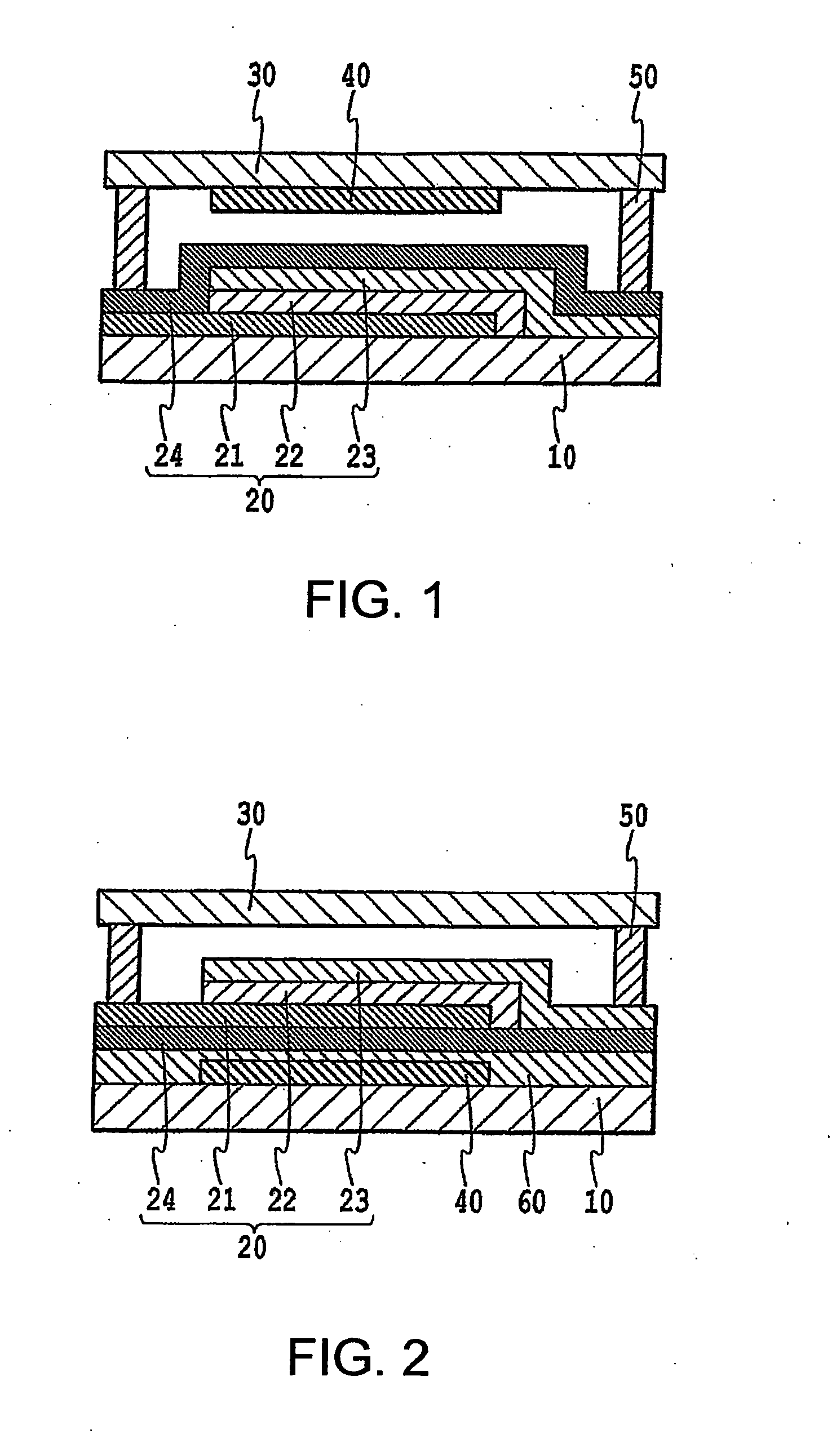
embodiment 1

[0086]In this embodiment, a red light-emitting organic EL device with 2×2 pixels, each pixel of size 0.3 mm×0.3 mm, was fabricated.

[0087]As the substrate, fusion glass (Corning 1737 glass, 50×50×1.1 mm) was prepared. A sputtering method was used to deposit Ag film to a thickness of 100 nm on the substrate. A photolithography method was used to pattern the Ag film obtained, to form two lower electrodes comprising stripe-shape electrodes of width 0.3 mm.

[0088]Next, the substrate with lower electrode formed was placed in a resistive-heating evaporation deposition device. By means of an evaporation deposition method using a mask, a buffer layer comprising Li, of film thickness 1.5 nm, was formed on the lower electrode 21. Then, evaporation deposition was used to form an organic EL layer, comprising four layers which were an electron transport layer / light-emitting layer / hole transport layer / hole injection layer. The electron transport layer was Alq3 of thickness 20 nm, the light-emitting...


PUM


Abstract

An organic EL device is provided and, in particular, a top-emission-type organic EL device, which can maintain excellent light emission efficiency over a prolonged period of time. The organic EL device includes a substrate; and an organic EL element that is formed on the substrate and that includes a lower electrode, an organic EL layer, an upper electrode, and a protective layer. The protective layer includes at least one inorganic film provided that at least one film thereof is a SiN:H film having a stretching-mode peak area ratio, as determined by infrared absorption spectrum measurements, of N—H bonds to Si—N bonds that is greater than 0.06 but does not exceed 0.1, and having a stretching-mode peak area ratio, as determined by infrared absorption spectrum measurements, of Si—H bonds to Si—N bonds that is greater than 0.12 but does not exceed 0.17.

Description

CROSS-REFERENCE TO RELATED APPLICATION(S)[0001]This non-provisional Application is the U.S. National Stage Application of Applicant's earlier filed PCT Application No. JP2008 / 063293, that was filed in Japan on Jul. 24, 2008, the entire contents of which are incorporated herein by reference.BACKGROUND OF THE INVENTION[0002]1. Field of the Invention[0003]This invention relates to an organic EL device which is useful for display applications, and to a method for manufacturing such a device. More specifically, this invention relates to an organic EL device which prevents intrusion of moisture from the outside environment, and exhibits excellent light emission efficiency over a long period of time, and to a method for manufacturing such a device.[0004]2. Description of the Related Art[0005]In recent years energetic research has been performed on organic EL devices employing light-emissive organic EL elements. Organic EL devices are expected to achieve high emission luminance and emission...

Claims


Application Information

Patent Timeline
IPC IPC(8): H01L51/50H01L51/40
CPCH01L27/322H01L51/524H05B33/10H01L2251/5315H05B33/04H01L51/5262H10K59/38H10K50/841H10K50/85H10K2102/3026H10K50/844
Inventor UTUMI, MAKOTO
Owner SHARP KK
Why Eureka
Try Eureka