Supercharge Your Innovation With Domain-Expert AI Agents!

CMOS image sensor with self-aligned photodiode implants

a self-aligning, photodiode technology, applied in the direction of semiconductor/solid-state device manufacturing, semiconductor devices, electrical equipment, etc., can solve the problems of limiting the full well capacity of the photodiode, accelerating the decline of the full well capacity, and adding complexity and cost to the standard cmos fabrication process

Inactive Publication Date: 2011-07-21
OMNIVISION TECH INC
View PDF2 Cites 17 Cited by
  • Summary
  • Abstract
  • Description
  • Claims
  • Application Information

AI Technical Summary

Problems solved by technology

This restriction on implanted depth may limit the full well capacity of the photodiode.
This solution however adds complexity and cost to a standard CMOS fabrication process.
This may result in an accelerated decline of the full well capacity and therefore a decline in performance of the pinned photodiode pixel.
A disadvantage of such a method is the use of two photoresist masks and the potential for performance reduction due to photomask misalignment.

Method used


Image

  • CMOS image sensor with self-aligned photodiode implants
  • CMOS image sensor with self-aligned photodiode implants
  • CMOS image sensor with self-aligned photodiode implants

Examples


Embodiment Construction

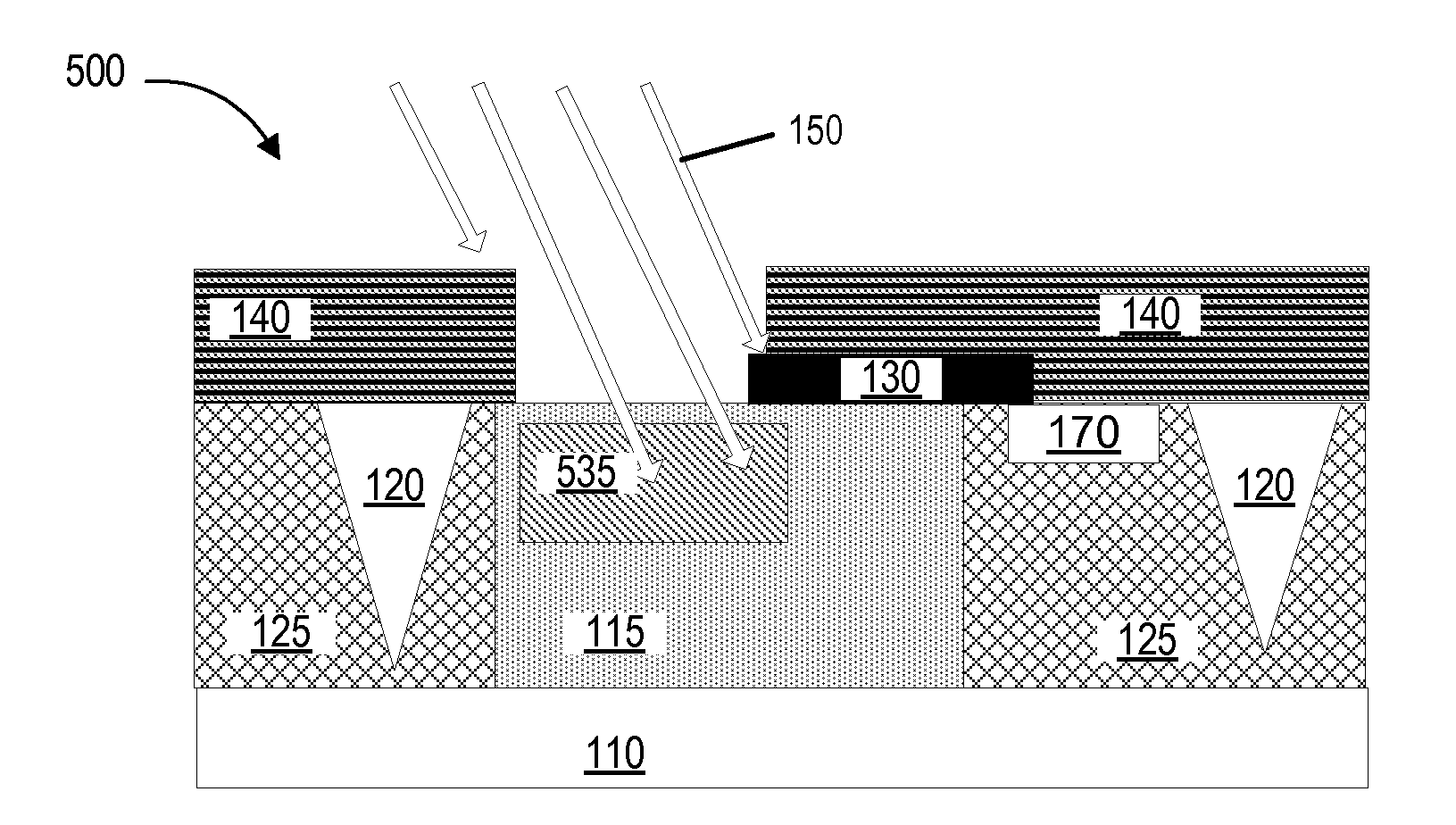
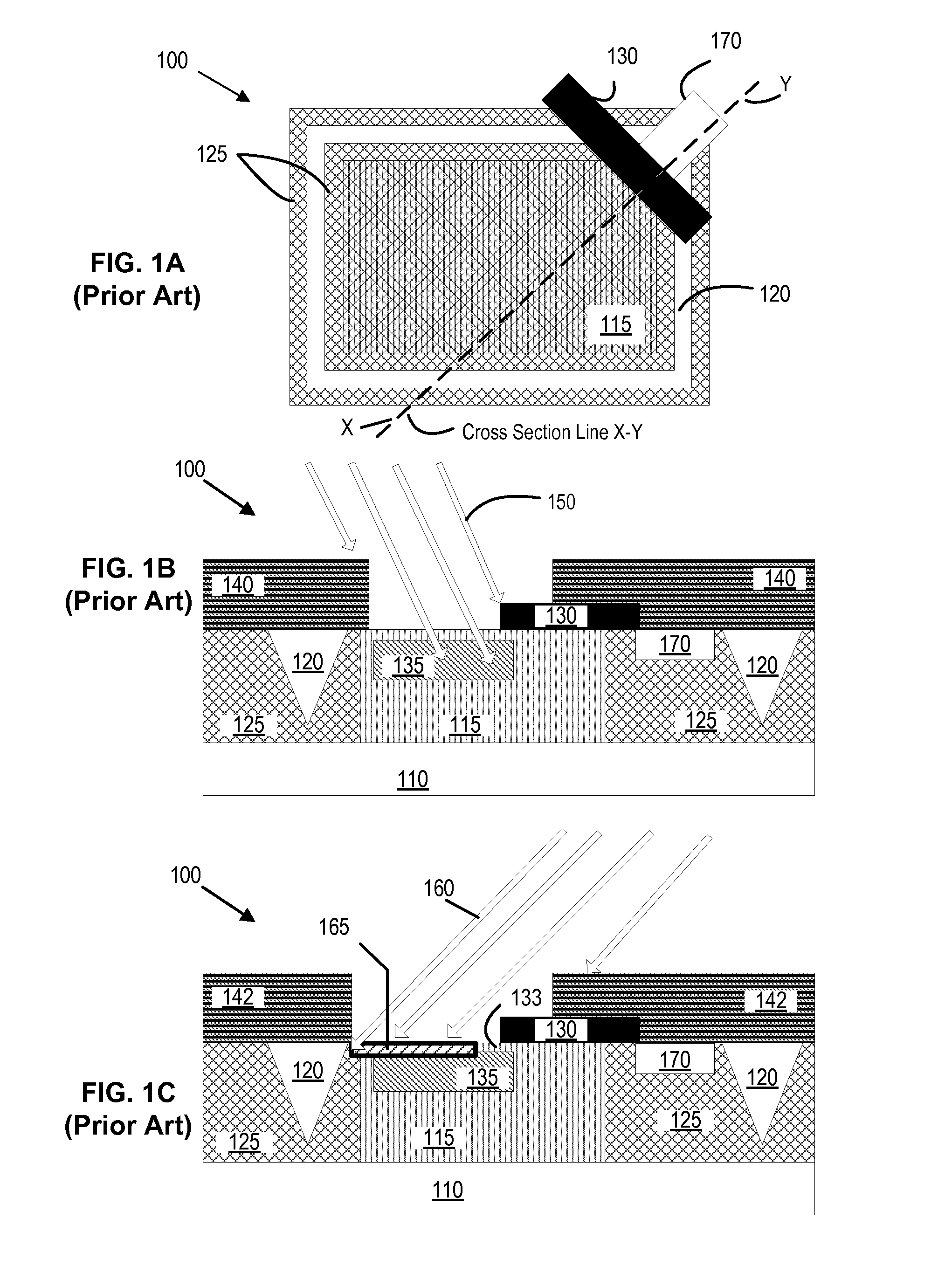
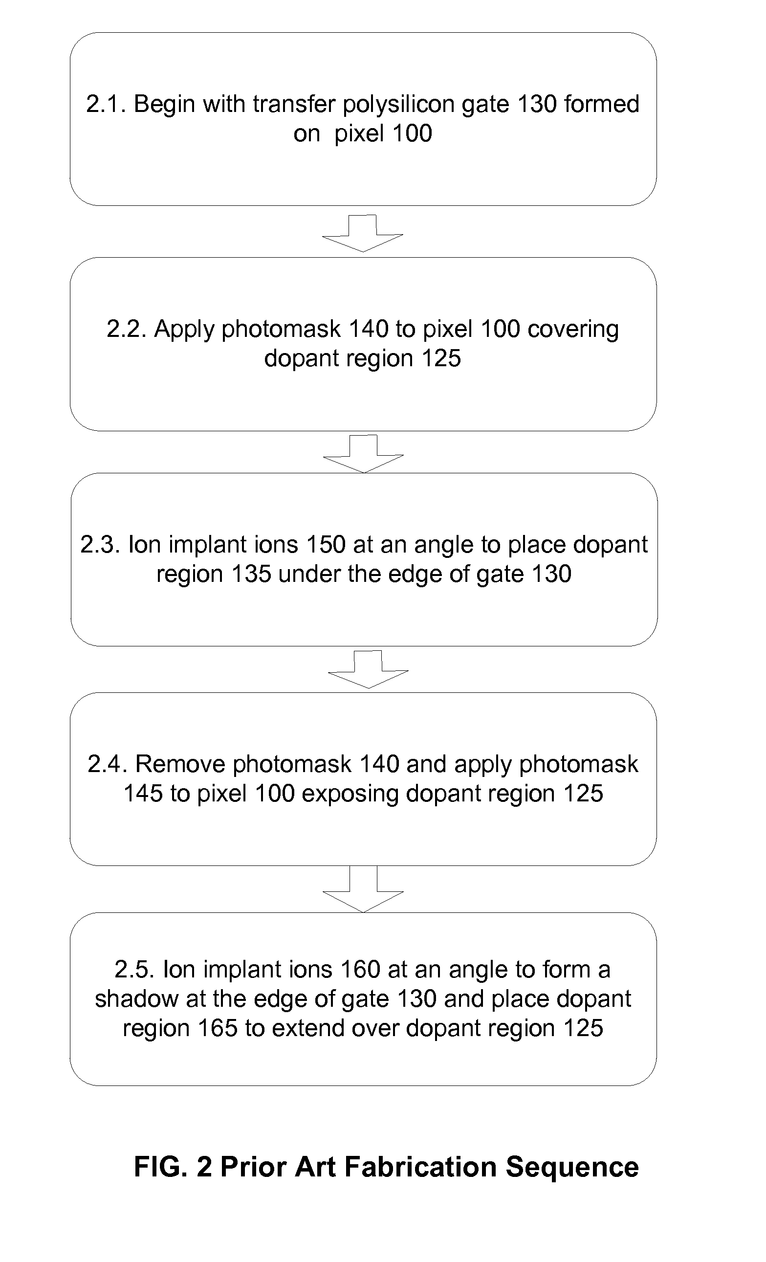
[0018]Embodiments of an image sensor array having self-aligned pinned photodiode implants and methods for its fabrication are described herein. In the following description numerous specific details are set forth to provide a thorough understanding of the embodiments. One skilled in the relevant art will recognize, however, that the techniques described herein can be practiced without one or more of the specific details, or with other methods, components, materials, etc. In other instances, well-known structures, materials, or operations are not shown or described in detail to avoid obscuring certain aspects.

[0019]Reference throughout this specification to “one embodiment” or “an embodiment” means that a particular feature, structure, or characteristic described in connection with the embodiment is included in at least one embodiment. Thus, the appearances of the phrases “in one embodiment” or “in an embodiment” in various places throughout this specification are not necessarily all...


PUM


Abstract

An example method of forming a pinned photodiode includes applying a photoresist mask to a semiconductor layer at a location where a transfer gate will subsequently be formed. First dopant ions are then implanted at a first angle to form a first dopant region under an edge of the photoresist mask. Next, a photoresist mask is etched such that a thickness of the photoresist mask is reduced to form a trimmed photoresist mask. Second dopant ions are then implanted at a second angle to form a second dopant region, wherein the second dopant ions are shadowed by the trimmed photoresist mask to exclude the second dopant ions from a region partially above the first dopant region and adjacent to an edge of the trimmed photoresist mask.

Description

TECHNICAL FIELD[0001]This disclosure relates to image sensing devices, and more particularly, to the integration of pinned photodiode technology within CMOS technology.BACKGROUND INFORMATION[0002]Integrated circuit implementations of imaging sensors may use active pixel arrays which have active devices, such as transistors, associated with each pixel. The active pixel sensor has the advantage of being able to incorporate both signal processing and sensing circuitry within the same integrated circuit. Conventional active pixel sensors typically employ silicon based CMOS transistor fabrication technology to form pinned photodiode sensors and adjacent transfer gates. The pinned photodiode has gained favor for its ability to have good color response for blue light, as well as advantages in dark current density and image lag. Reduction of dark current is accomplished by pinning the diode surface potential to a p type doped well or p type doped substrate (GND) through a p type doped well ...

Claims


Application Information

Patent Timeline
IPC IPC(8): H01L31/18H01L21/265
CPCH01L21/26586H01L27/14689H01L27/1461
Inventor QIAN, YINTAI, HSIN-CHIHMAO, DULIVENEZIA, VINCENTRHODES, HOWARD E.
Owner OMNIVISION TECH INC
Features
  • R&D
  • Intellectual Property
  • Life Sciences
  • Materials
  • Tech Scout
  • Unparalleled Data Quality
  • Higher Quality Content
  • 60% Fewer Hallucinations
Learn More