Method of thin film epitaxial growth using atomic layer deposition

a thin film and atomic layer technology, applied in the direction of crystal growth process, chemically reactive gas, coating, etc., can solve the problems of high consumption of deposition precursors, difficult pulsing of molecular precursors to uniformly fill high aspect ratio features on the substrate in a short time, and inconvenient ald process for epitaxial growth

Active Publication Date: 2011-07-21
NAT SYNCHROTRON RADIATION RES CENT
View PDF3 Cites 6 Cited by
  • Summary
  • Abstract
  • Description
  • Claims
  • Application Information

AI Technical Summary

Benefits of technology

[0006]The present invention is directed to providing a method of thin film epitaxial growth using atomic layer deposition. The method introduces deposition precursors into a chamber after a vent valve connected between the chamber and a vacuum pump is closed, thereby reducing the consumption of deposition precursor and realizing a thin film epitaxial growth on the substrate.

Problems solved by technology

The conventional ALD process is not suitable for epitaxial growth and for thin films having preferred orientation because the partial pressure of the deposition precursor in the chamber is not stable and a substrate within the chamber is not in thermal equilibrium while reacting with the deposition precursor.
Furthermore, pulsing molecular precursors to uniformly fill high aspect ratio features on the substrate in a short time is difficult because there is no sufficient time for deposition precursors to diffuse to the deep surface on the substrate effectively.
Although a conventional ALD method is proposed to resolve the aforementioned issues by extending the time for introducing deposition precursors into the chamber, the resulting deposition precursor consumption is high because most of deposition precursors have not reacted with the substrate before being removed by a vacuum pumping system.

Method used


Image

  • Method of thin film epitaxial growth using atomic layer deposition
  • Method of thin film epitaxial growth using atomic layer deposition
  • Method of thin film epitaxial growth using atomic layer deposition

Examples


Embodiment Construction

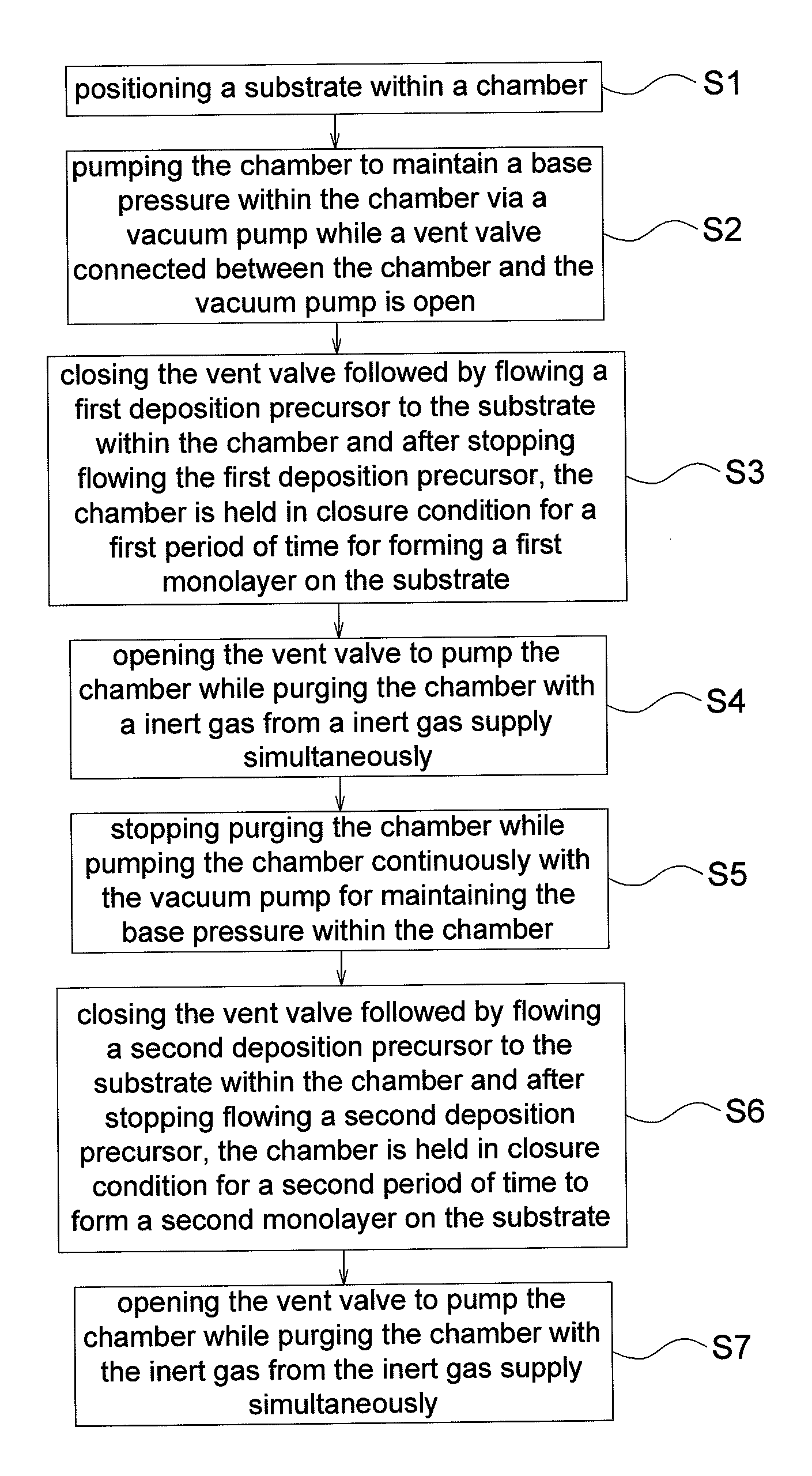
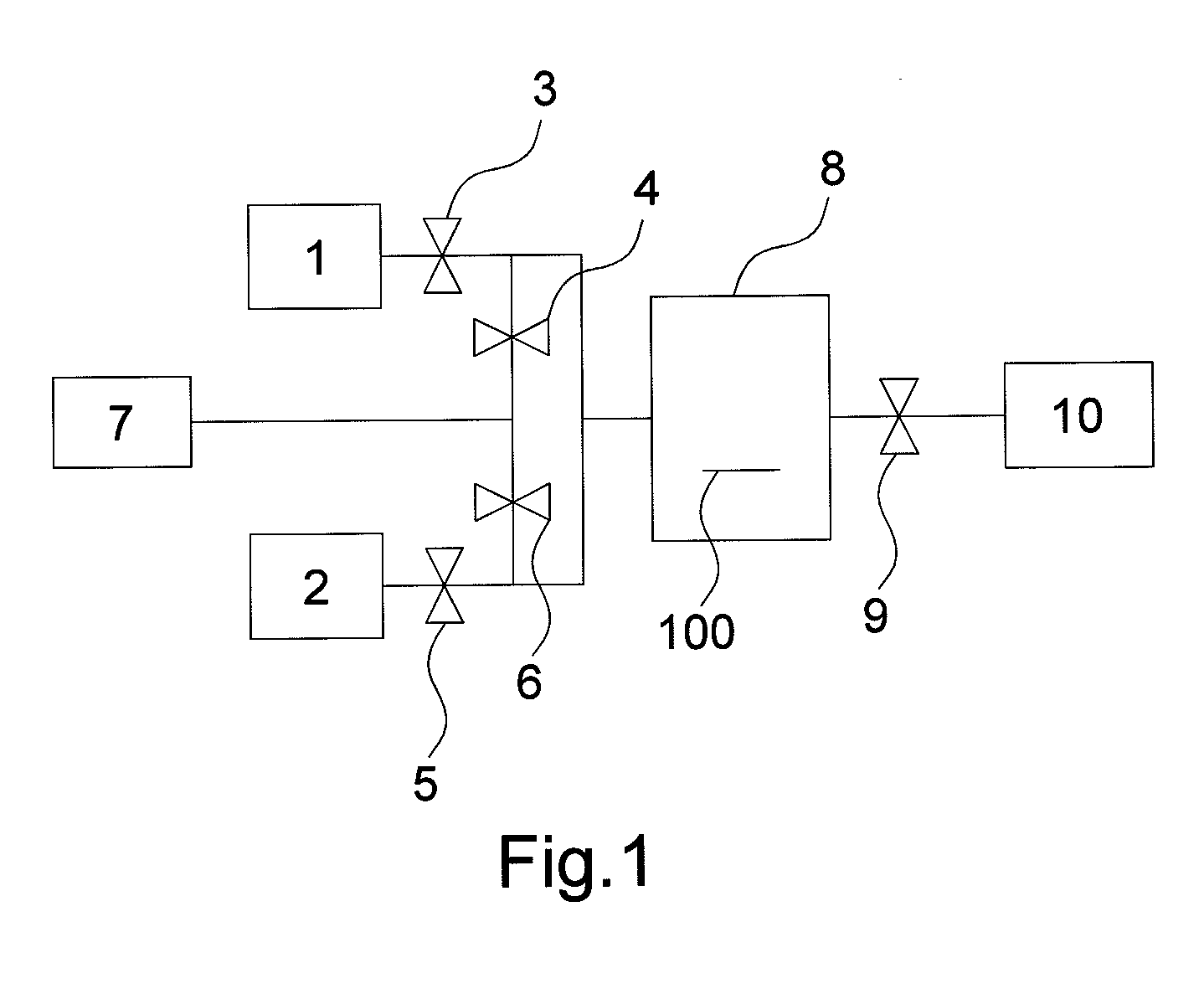
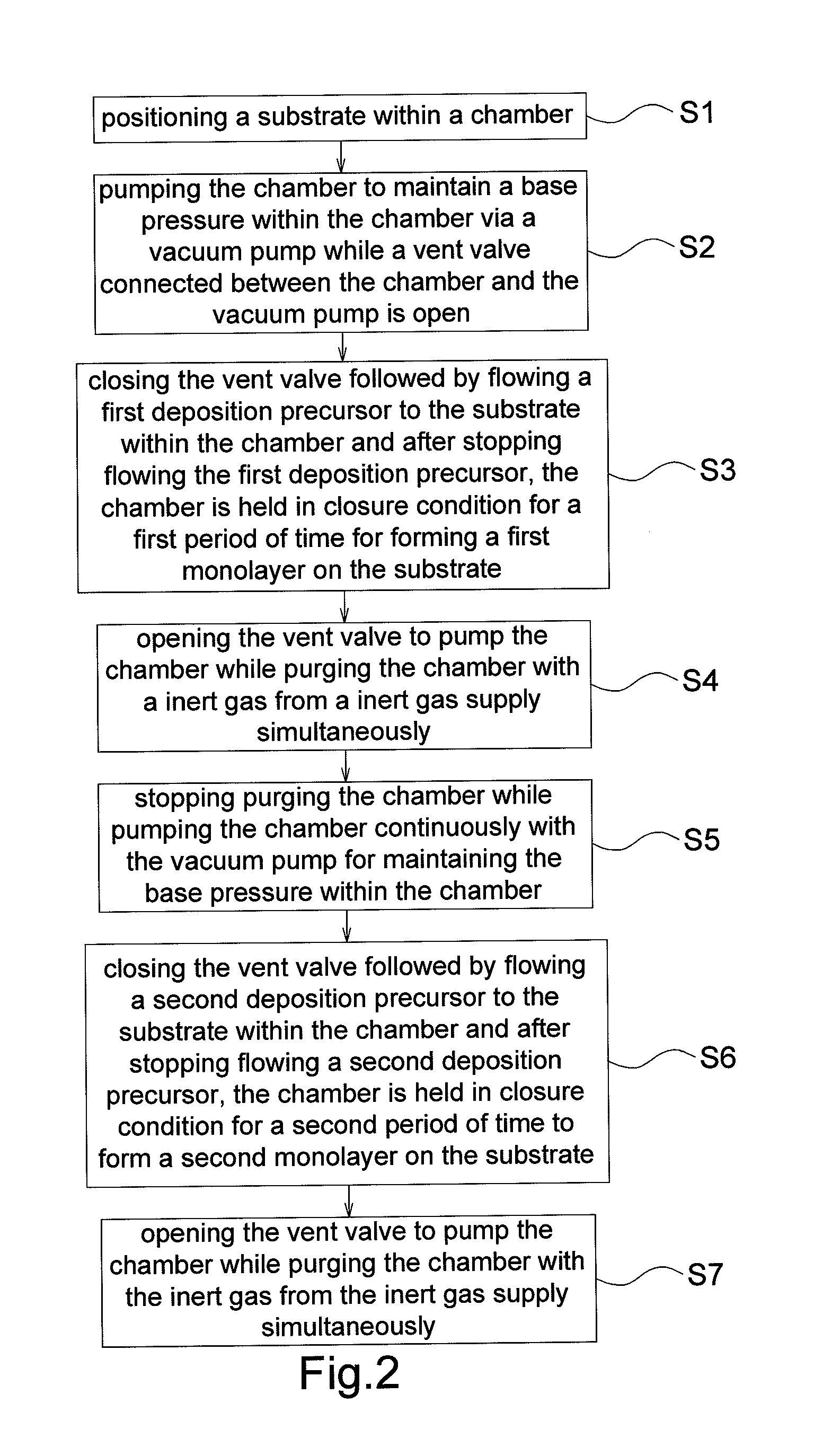
[0015]Referring to FIG. 1, FIG. 1 is a schematic diagram of an atomic layer deposition (ALD) apparatus. As shown in FIG. 1, the ALD apparatus comprises an inert gas supply 7, a chamber 8, a vacuum pump 10, a first deposition precursor supply 1, a second deposition precursor supply 2, a vent valve 9, four two-port solenoid valves 3, 4, 5, 6 and a manifold 11 having two inlets and one outlet. A first deposition precursor and a second deposition precursor is contained in the first deposition precursor supply 1 and the second deposition precursor supply 2 respectively. The vent valve 9 is connected between the chamber 8 and the vacuum pump 10 for the vacuum pump 10 to vacuum the chamber 8 or remove gaseous species (e.g. unreacted precursor, reaction products, etc.).

[0016]The two-port solenoid valve 3 is connected between the first deposition precursor supply 1 and one inlet of the manifold 11; the two-port solenoid valve 5 is connected between the second deposition precursor supply 2 an...


PUM

PropertyMeasurementUnit
pressureaaaaaaaaaa
pressureaaaaaaaaaa
temperatureaaaaaaaaaa

Abstract

A method of thin film epitaxial growth using atomic layer deposition is provided by introducing a first deposition precursor and a second deposition precursor into a chamber after a vent valve connected between the chamber and a vacuum pump is closed. The chamber is maintained in a thermal equilibrium state and a constant pressure as a result of keeping the first deposition precursor and the second deposition precursor inside the chamber thereby reducing deposition precursors consumption and achieving thin film epitaxial growth on the substrate.

Description

BACKGROUND OF THE INVENTION[0001]1. Field of the Invention[0002]The present invention relates to a method of thin film growth and more particularly to a method of thin film epitaxial growth using atomic layer deposition.[0003]2. Description of the Prior Art[0004]Atomic layer deposition (ALD) is a technique that allows growth of thin films. For a conventional ALD application, each deposition precursor is alternately pulsed into a carrier gas stream which continuously flows into an ALD chamber and an inert purge gas is introduced into the ALD chamber between each deposition precursor pulse to evacuate the ALD chamber. The conventional ALD process is not suitable for epitaxial growth and for thin films having preferred orientation because the partial pressure of the deposition precursor in the chamber is not stable and a substrate within the chamber is not in thermal equilibrium while reacting with the deposition precursor.[0005]Furthermore, pulsing molecular precursors to uniformly fi...

Claims


Application Information

Patent Timeline
Patent Type & Authority Applications(United States)
IPC IPC(8): H01L21/20H01L21/36
CPCC23C16/407C23C16/45525H01L21/02554H01L21/0242C30B25/165
Inventor KU, CHING-SHUN
Owner NAT SYNCHROTRON RADIATION RES CENT
Why Eureka
Try Eureka