Model based simulation and optimization methodology for design checking

Active Publication Date: 2011-07-28
GLOBALFOUNDRIES US INC
View PDF8 Cites 9 Cited by
  • Summary
  • Abstract
  • Description
  • Claims
  • Application Information

AI Technical Summary

Benefits of technology

[0006]Therefore there is a need in the art to improve upo

Problems solved by technology

In general, an input / output circuit design may be very complex and involve difficult compromises between performance (e.g., speed or data rate) and electrostatic discharge (ESD) protection.
After testing, it may be determined that the selected ESD protection device was not optimum for the desired application, such as for example being too large or in an incorrect configuration, and the process would have to be repeated such as by selecting another ESD protection device or reconfiguring the current design for further testing.
In general, this approach is time consuming and expensive with results that are often difficult to predict.
However, contemporary simulations may run for long periods of time, providing little or no information to the Design Engineer until the simulations are complete and then require a manual interpretation of the simulation results to identify critical parameters and / or critical paths.
After analyzing the results, the Design Engineer may then go back to the design and make changes based on feedback from the results, though results traditionally only provide worst case scenarios and the Design Engineer has little insight as to where the next problem or critical area in the design may lie.

Method used


Image

  • Model based simulation and optimization methodology for design checking
  • Model based simulation and optimization methodology for design checking
  • Model based simulation and optimization methodology for design checking

Examples


Embodiment Construction

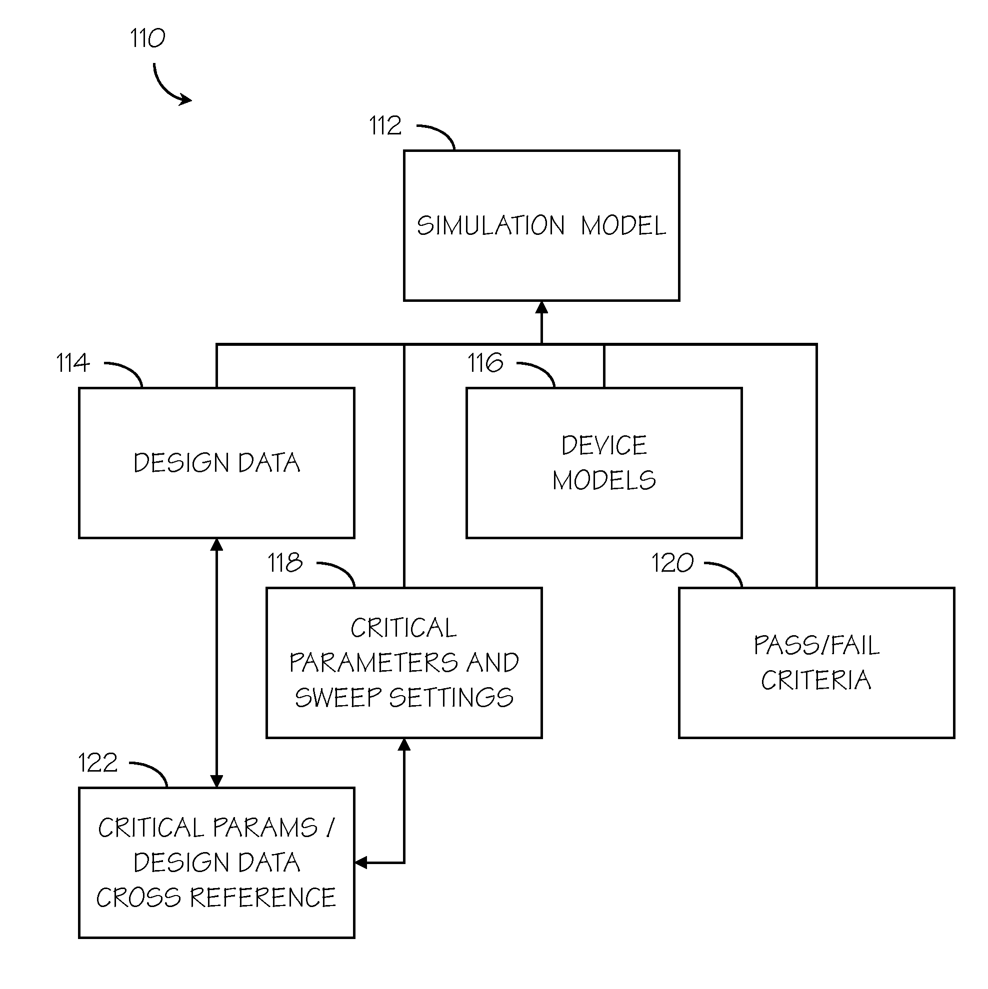
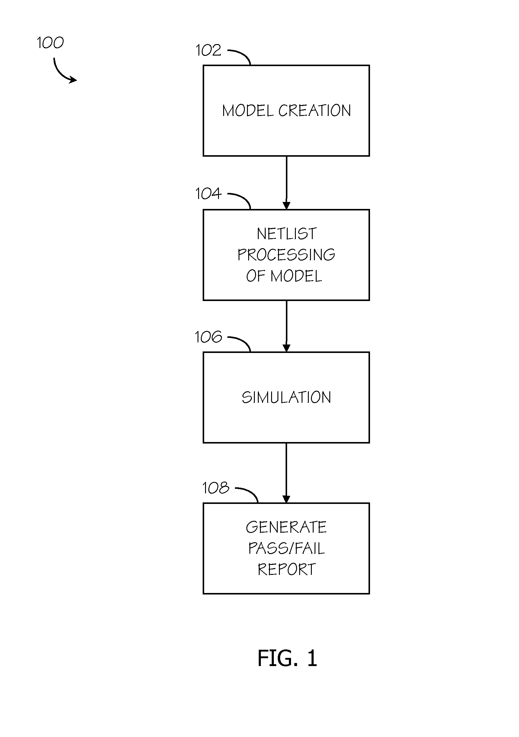
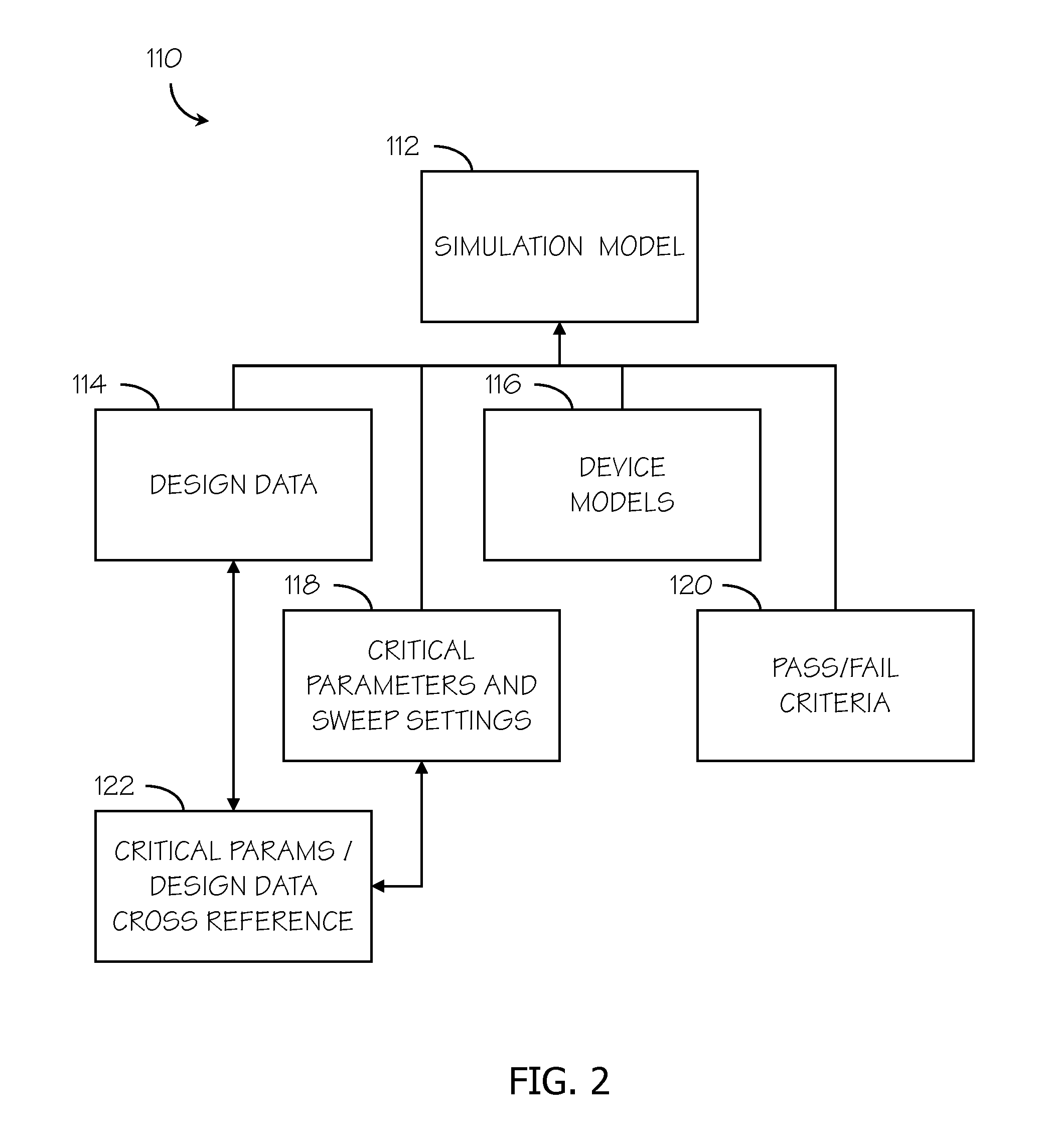
[0022]Embodiments of the invention enable Design Engineers to use simulation-based I / O circuit design in order to achieve satisfactory ESD protection levels earlier in the design process. Based on the fragile nature and ever growing number of devices on chips, there is a need for chip protection. Many contemporary practices do not employ simulation, but rather trial and error approaches, and historically only ESD ground rules and ESD device data are provided for customer use. However, accurate ESD prediction requires accurate ESD high current models for ESD transient event simulation.

[0023]Embodiments of the invention assist in enabling ESD simulation-based checking tools for use with ESD protection circuit design and verification. Embodiments may also provide the capability of using industry standard circuit simulators, such as SPICE, or even internally developed circuit simulators to qualify cell libraries and to predict ESD chip failure. ESD compact model simulations along with E...


PUM


Abstract

A method, apparatus and program product are provided for simulating a circuit. A plurality of elements of the circuit is represented by device models including pass / fail criteria. A circuit simulation program is executed on a hardware implemented processor where the circuit simulation program is configured to obtain simulation results from the device models in response to applied parameters. The circuit simulation program identifies a failure of one or more of the plurality of elements of the circuit based on the pass / fail criteria of the device models. The circuit simulation program is further configured to output the failures during simulation of the one or more of the plurality of elements that are identified in response to the applied parameters.

Description

BACKGROUND[0001]The present invention relates generally to electrical circuits, and more specifically, to the simulation of electrostatic discharge.[0002]A modern integrated circuit may communicate by utilizing a number of different input and output signal standards. For example, an integrated circuit may transmit and receive information via one or more input / output circuits, which may be within the same input / output bank, at high speeds (e.g. 1 Gpbs). The input / output circuit typically must also be designed to be protected from (e.g., have a certain immunity to damage from) electrostatic discharge.[0003]In general, an input / output circuit design may be very complex and involve difficult compromises between performance (e.g., speed or data rate) and electrostatic discharge (ESD) protection. For example, a typical input / output circuit design process may involve adding standard, pre-approved ESD protection devices to the input / output circuit. The ESD protection device and the input / ou...

Claims


Application Information

Patent Timeline
IPC IPC(8): G06F17/50
CPCG06F17/5036G06F30/367
Inventor GAUTHIER, JR., ROBERT J.HUNTER, BRADFORD L.JOSHI, AMOL A.LI, JUNJUNSCHROER, GREGORY JOSEPH
Owner GLOBALFOUNDRIES US INC
Why Eureka
Try Eureka