Light-emitting device, illumination apparatus, and display apparatus

a technology of illumination apparatus and light-emitting device, which is applied in the direction of electric discharge tube, electric discharge lamp, incandescent envelope/vessel, etc., can solve the problems of increasing the dependence of viewing angle of emission characteristics, difficult to obtain white emission having a wide spectrum, and difficult to achieve phase cancellation, etc., to reduce the dependence of luminance and hue, reduce the dependence of viewing angle, and achieve the effect of extracting light in a wide wavelength rang

Inactive Publication Date: 2011-08-04
SONY CORP
View PDF3 Cites 39 Cited by
  • Summary
  • Abstract
  • Description
  • Claims
  • Application Information

AI Technical Summary

Benefits of technology

[0056]According to the embodiments of the present invention, it is possible to realize providing a light-emitting device capable of effectively extracting light in a wide wavelength range and greatly reducing a viewing-angle dependency of luminance and hue with respect to light of a single color or a combined color of two or more diff...

Problems solved by technology

Thus, the viewing-angle dependency of emission characteristics increases.
When the emission position is separated from the reflective layer and the distance increases, it is difficult to obtain white emission having a wide spectrum due to the interference.
However, since it is difficult to achieve phase cancellation over a wide wavelength ran...

Method used


Image

  • Light-emitting device, illumination apparatus, and display apparatus
  • Light-emitting device, illumination apparatus, and display apparatus
  • Light-emitting device, illumination apparatus, and display apparatus

Examples


first embodiment

1. First Embodiment

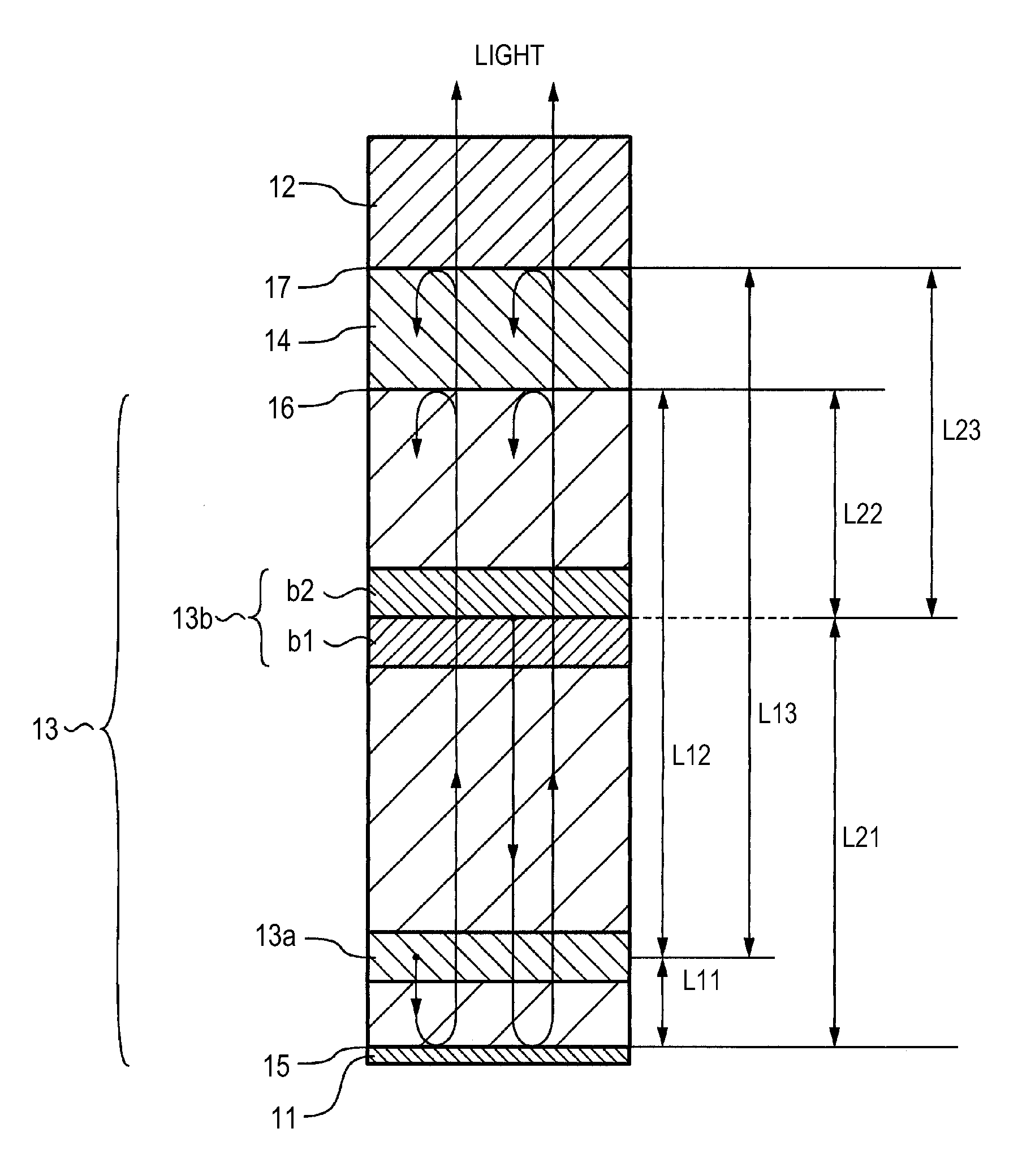
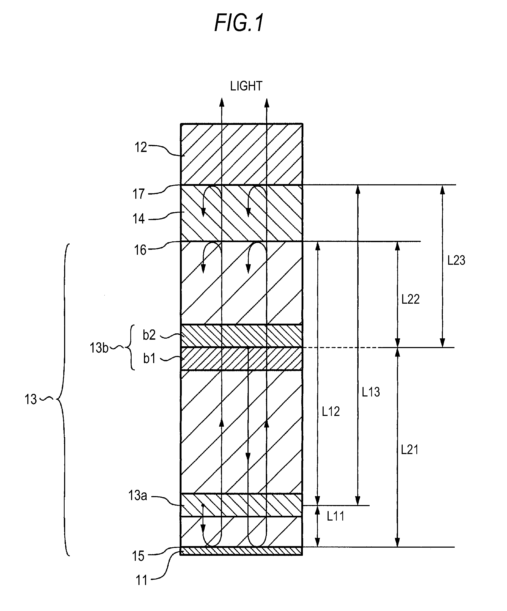
[0080]FIG. 1 shows an organic EL device according to a first embodiment.

[0081]As shown in FIG. 1, in this organic EL device, an organic layer 13 is interposed between a first electrode 11 and a second electrode 12, in which a first light-emitting layer 13a and a second light-emitting layer 13b are sequentially included in the organic layer 13 at mutually separated positions in that order in the direction from the first electrode 11 to the second electrode 12. Like the existing organic EL device, a hole injection layer, a hole transport layer, an electron transport layer, an electron injection layer, and the like, as necessary, are formed in portions of the organic layer 13 above or under the first light-emitting layer 13a and above or under the second light-emitting layer 13b. In this case, the second electrode 12 is a transparent electrode that transmits visible light, and light is emitted from the side of the second electrode 12. The first light-emitting layer 1...

second embodiment

2. Second Embodiment

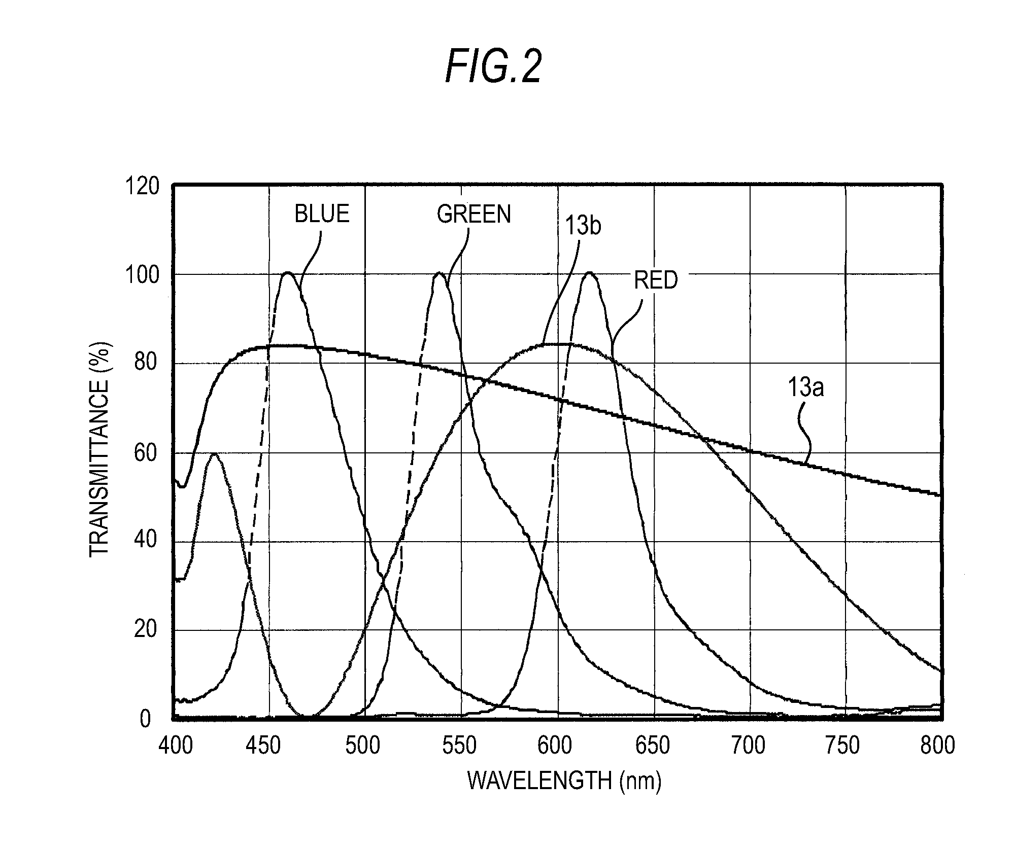
[0098]In an organic EL device according to a second embodiment, the second and third reflective interfaces 16 and 17 of the organic EL device according to the first embodiment are respectively divided into two front and rear reflective interfaces so as to broaden the wavelength range of the opposite-phase interference conditions shown in the expressions (3) to (6). That is, as for the expression (3), for example, when the second reflective interface 16 is divided into two front and rear reflective interfaces separated by a distance of Δ, L12 becomes L12+Δ and L12−Δ, the wavelength range of λ12 in which the expression (3) is satisfied is broadened. The same applies to the expressions (4) to (6).

[0099]According to the second embodiment, in addition to the same advantages as the first embodiment, since the wavelength range of the opposite-phase interference condition shown in the expressions (3) to (6) can be broadened, it is possible to obtain an advantage that the...

third embodiment

3. Third Embodiment

[0100]In the organic EL device according to the first embodiment, there is a case where the portions of the light-emitting layers b1 and b2 of the second light-emitting layer 13b are formed by a stacked structure made up of a plurality of layers depending on a manufacturing method of the organic EL device or in order to obtain necessary properties. Thus, the portions become thick. Moreover, as for the stacking order of the green light-emitting layer b1 and the red light-emitting layer b2, it is preferable to stack the layers in the descending order of the emission wavelength from the side of the first electrode 11. That is, the green light-emitting layer b1 and the red light-emitting layer b2 are preferably stacked in that order from the side of the first electrode 11 similarly to the first embodiment. However, the stacking order of the green light-emitting layer b1 and the red light-emitting layer b2 may be reversed. In such a case, since it is difficult to regar...


PUM


Abstract

A light-emitting device including: an organic layer which is interposed between a first electrode and a second electrode and in which a first light-emitting layer and a second light-emitting layer emitting light of single colors or two or more different colors in a visible wavelength region are sequentially included at mutually separated positions in that order in a direction from the first electrode to the second electrode; a first reflective interface which is provided on the side of the first electrode so as to reflect light emitted from the first light-emitting layer and the second light-emitting layer to be emitted from the side of the second electrode; and a second reflective interface and a third reflective interface which are sequentially provided on the side of the second electrode at mutually separated positions in that order in a direction from the first electrode to the second electrode.

Description

BACKGROUND OF THE INVENTION[0001]1. Field of the Invention[0002]This invention relates to a light-emitting device, an illumination apparatus, and a display apparatus. More specifically, the invention relates to a light-emitting device which uses electroluminescence of an organic material, and an illumination apparatus and a display apparatus using the light-emitting device.[0003]2. Description of the Related Art[0004]Light-emitting devices (hereinafter referred to as organic EL devices) which use electroluminescence of an organic material have attracted attention as a light-emitting device capable of emitting high-luminance light with low-voltage direct-current driving and have been actively researched and developed. The organic EL device has a structure in which an organic layer having a light-emitting layer that generally has a thickness of about several tens to several hundreds of nm is interposed between a reflective electrode and a translucent electrode. In such an organic EL d...

Claims


Application Information

Patent Timeline
IPC IPC(8): H01K1/26
CPCH01K1/26H10K50/19H10K59/876H10K50/852
Inventor FUKUDA, TOSHIHIROYAMADA, JIROEBIHARA, YOHEI
Owner SONY CORP
Why Eureka
Try Eureka