Method for manufacturing semiconductor device

a semiconductor and manufacturing technology, applied in solid-state devices, liquid/solution decomposition chemical coatings, coatings, etc., can solve the problems of poor conduction or poor appearance, poor appearance, and low yield, and achieve poor appearance, poor conduction, and poor yield.

Active Publication Date: 2011-08-11
MITSUBISHI ELECTRIC CORP
View PDF1 Cites 16 Cited by
  • Summary
  • Abstract
  • Description
  • Claims
  • Application Information

AI Technical Summary

Benefits of technology

[0007]However, by conventional methods using vapor deposition or sputtering, the thickness of the metal film on the sidewall of the via hole was several percent the thickness on flat portions. Therefore, the lowering of yield due to poor conduction caused problems. Also in the case of performing Au electrolytic plating using the metal film formed by vapor deposition or sputtering as the power supply layer, the Au-plated film was not grown or abnormally grown in the via hole causing poor conduction or poor appearance, and also causing lower yield.

Problems solved by technology

Therefore, the lowering of yield due to poor conduction caused problems.
Also in the case of performing Au electrolytic plating using the metal film formed by vapor deposition or sputtering as the power supply layer, the Au-plated film was not grown or abnormally grown in the via hole causing poor conduction or poor appearance, and also causing lower yield.

Method used


Image

  • Method for manufacturing semiconductor device
  • Method for manufacturing semiconductor device
  • Method for manufacturing semiconductor device

Examples


first embodiment

[0023]A method for manufacturing a semiconductor device according to the first embodiment of the present invention will be described. FIGS. 4 to 12 are sectional views for illustrating the method for manufacturing a semiconductor device according to the first embodiment.

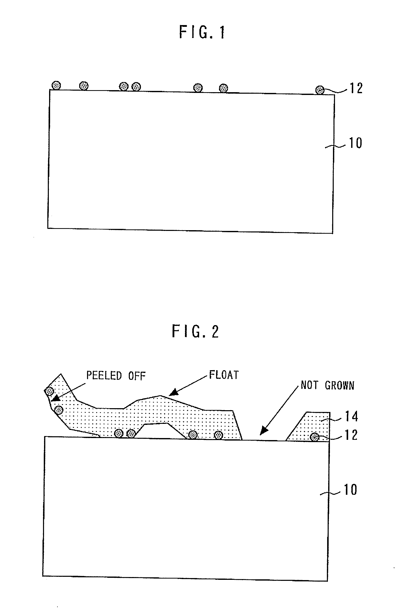
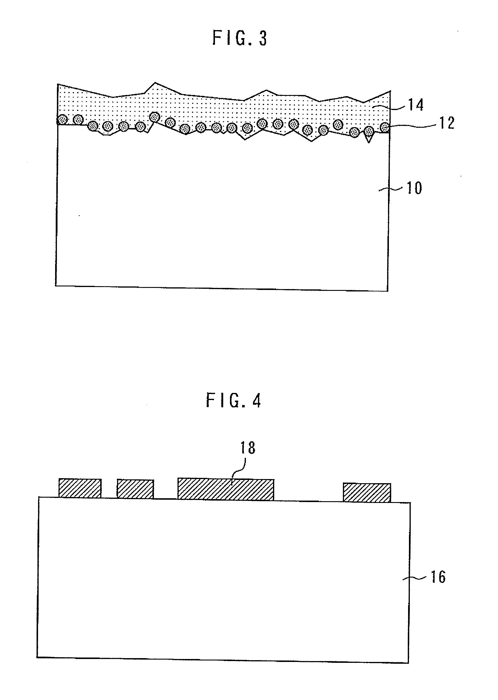
[0024]First, as shown in FIG. 4, devices, such as an electrode 18 and a transistor (not shown) are formed on the upper surface of a GaAs substrate 16 (semiconductor substrate). Then, as shown in FIG. 5, the device forming surface (upper surface) of the GaAs substrate 16 is adhered to a sapphire support substrate 22 having a thickness of about 1 mm by an adhesive 20, such as wax and an adhesive tape. In such a state, the back surface of the GaAs substrate 16 is polished to thin the GaAs substrate 16.

[0025]Next, as shown in FIG. 6, the GaAs substrate 16 is etched from the back surface side. Thereby, a via hole 24 is formed through the GaAs substrate 16 from the back surface of the GaAs substrate 16 to the back surface ...

second embodiment

[0042]A method for manufacturing a semiconductor device according to the second embodiment will be described referring to the drawings. FIG. 16 is a top view for illustrating the method for manufacturing the semiconductor device according to the second embodiment; and FIG. 17 is a sectional view thereof.

[0043]First, a bump 54 is formed on a GaAs substrate 16 (semiconductor substrate) by etching. Next, in the same manner as in the first embodiment, a Pd-plated film 44 is formed on the flat portion and the side portion of the bump 54 on the GaAs substrate 16. Thus, a Pd film can be uniformly formed on the surface of the semiconductor substrate having the dump. For example, wirings or electrode pads across the bump can be formed without disconnecting or narrowing.


PUM

PropertyMeasurementUnit
temperatureaaaaaaaaaa

Abstract

A method for manufacturing a semiconductor device comprises: immersing a semiconductor substrates in a Pd activating solution containing Pd ions and adhering a Pd catalyst to a surface of the semiconductor substrate; and immersing the semiconductor substrate, to which the Pd catalyst is adhered, in a Pd electroless plating solution and forming an electroless-plated Pd film on the semiconductor substrate.

Description

BACKGROUND OF THE INVENTION[0001]1. Field of the Invention[0002]The present invention relates to a method for manufacturing a semiconductor device that can form the metal film having high coating characteristics and adhesion on the semiconductor substrate at low costs.[0003]2. Background Art[0004]When electrodes other than an ohmic electrode are formed on a semiconductor substrate, generally, two layers or more metal films are often formed using vapor deposition, sputtering or the like. For the upper layer, a material having high electric conductivity, whose surface is hard to be oxidized, such as Au, is used. In place of Au, Ag, Cu or the like may be used. The lower layer is a barrier layer that prevents the diffusion of Au into the semiconductor substrate. As the barrier layer, Ti, TiN, TaN, Pt or the like is often used. Furthermore, in order to secure required current, these layers may be subjected to Au electrolytic plating as power supply layers. In place of Au electrolytic pla...

Claims


Application Information

Patent Timeline
Patent Type & Authority Applications(United States)
IPC IPC(8): H01L21/768H01L21/3205
CPCC23C18/1642C23C18/168C23C18/1692C23C18/1872C23C18/1879H01L2221/6834C23C18/44H01L21/288H01L21/6835H01L21/76898H01L29/452C23C18/42
Inventor NISHIZAWA, KOICHIRO
Owner MITSUBISHI ELECTRIC CORP
Why Eureka
Try Eureka