Method to fabricate small dimension devices for magnetic recording applications

Active Publication Date: 2011-08-18
HEADWAY TECH INC
View PDF12 Cites 34 Cited by
  • Summary
  • Abstract
  • Description
  • Claims
  • Application Information

AI Technical Summary

Benefits of technology

[0007]One objective of the present invention is to provide a method for shrinking sensor

Problems solved by technology

However, both of these methods have practical limits and cannot reproducibly generate a CD less than about 50 nm which is needed in high performance recording devices.
However, this reference does not address any detrimental effect the

Method used


Image

  • Method to fabricate small dimension devices for magnetic recording applications
  • Method to fabricate small dimension devices for magnetic recording applications
  • Method to fabricate small dimension devices for magnetic recording applications

Examples


example 1

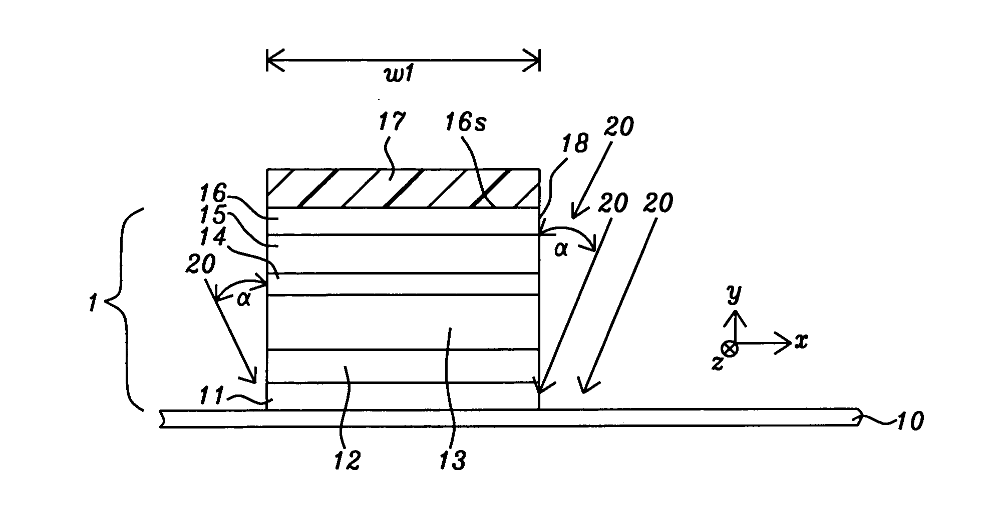
[0037]In order to demonstrate the benefits of the multiple step IBE sequence of the present invention, a TMR sensor was fabricated according to a method previously practiced by the inventors, and according to an embodiment as described herein. For each of the wafers 1, 2, and 3, a bottom spin valve configuration was formed on a AlTiC substrate and is represented by Ru / Ta / IrMn / CoFe / Ru / CoFeB / MgO / CoFeB / Ru / Ta where Ru / Ta is the seed layer, IrMn is the AFM layer, CoFe / Ru / CoFeB is the pinned layer, MgO is a tunnel barrier layer, CoFeB is the free layer, and Ru / Ta is a composite capping layer. Data was collected for circular shaped devices as described below.

[0038]Wafer 3 is a reference sample that is a sensor made by a prior art method in which the FLW formed after pattern transfer through the sensor stack of layers is trimmed with a single IBE step comprising an incident angle of 8 degrees with respect to a plane formed perpendicular to the substrate. As shown in Table 1, the sensor on w...


PUM

PropertyMeasurementUnit
Fractionaaaaaaaaaa
Fractionaaaaaaaaaa
Fractionaaaaaaaaaa

Abstract

A three step ion beam etch (IBE) sequence involving low energy (<300 eV) is disclosed for trimming a sensor critical dimension (free layer width=FLW) to less than 50 nm. A first IBE step has a steep incident angle with respect to the sensor sidewall and accounts for 60% to 90% of the FLW reduction. The second IBE step has a shallow incident angle and a sweeping motion to remove residue from the first IBE step and further trim the sidewall. The third IBE step has a steep incident angle to remove damaged sidewall portions from the second step and accounts for 10% to 40% of the FLW reduction. As a result, FLW approaching 30 nm is realized while maintaining high MR ratio of over 60% and low RA of 1.2 ohm-μm2. Sidewall angle is manipulated by changing one or more ion beam incident angles.

Description

FIELD OF THE INVENTION[0001]The invention relates to a method of trimming the critical dimension (CD) of a magnetoresistive sensor, and in particular, to a multi-step ion beam etch (IBE) process for trimming the sidewall of a giant magnetoresistive (GMR) element or a tunneling magnetoresistive (TMR) element while maintaining a high magnetoresistive ratio (dR / R) and other magnetic properties.BACKGROUND OF THE INVENTION[0002]A magnetic tunnel junction (MTJ) element also referred to as a sensor is a key component of magnetic recording devices. There is a continuous push to increase recording density which requires the sensor to become smaller in order to meet high performance demands of new devices. There are several ways to generate sensors with a smaller CD. One is to reduce the CD by shrinking the mask dimension in the pattern that is printed into a photoresist mask layer. Subsequently, the mask pattern is transferred through a MTJ stack of layers with an etch process to produce a p...

Claims


Application Information

Patent Timeline
IPC IPC(8): B44C1/22
CPCB82Y25/00G01R33/098G11B5/3163G11B5/398Y10T29/49021H01F41/308H01L43/12H01F10/3259B82Y40/00H01F10/3254H10N50/01
Inventor WANG, HUI-CHUANZHAO, TONGZHENG, MINYU, MINGHUILI, MINHAN, CHERNG CHYI
Owner HEADWAY TECH INC
Why Eureka
Try Eureka