Display device substrate, display device substrate manufacturing method, display device, liquid crystal display device, liquid crystal display device manufacturing method and organic electroluminescent display device

a technology of display device and substrate, which is applied in the direction of photomechanical equipment, instruments, photomechanical treatment originals, etc., can solve the problems of increasing aperture ratio, affecting the effect of display device performance, and generating drop in light transmittance during white display, etc., to achieve the effect of suppressing faults

Active Publication Date: 2011-08-18
SHARP KK
View PDF13 Cites 60 Cited by
  • Summary
  • Abstract
  • Description
  • Claims
  • Application Information

AI Technical Summary

Benefits of technology

[0067]The display device substrate, display device substrate manufacturing method, display device, liquid crystal display device, liquid crystal display device manufacturing method and organic electroluminescent display device of the present invention allow suppressing faults caused by generation of gas and / or formation of bubbles in a pixel region.

Problems solved by technology

However, in MVA mode liquid crystal display devices, a drop in light transmittance during white display tends to be generated at the boundaries between domains, for instance at regions where linear protrusions or slits are provided in the pixels.
MVA mode liquid crystal display devices, however, are provided with an alignment regulating structure, and hence an aligning treatment by rubbing is ordinarily not carried out.
Such a canister-sealed structure, however, makes it difficult to adopt top-emission structure in which light is extracted from the top face of the panel (increase in aperture ratio), and to realize thin-profile panels.

Method used


Image

  • Display device substrate, display device substrate manufacturing method, display device, liquid crystal display device, liquid crystal display device manufacturing method and organic electroluminescent display device
  • Display device substrate, display device substrate manufacturing method, display device, liquid crystal display device, liquid crystal display device manufacturing method and organic electroluminescent display device
  • Display device substrate, display device substrate manufacturing method, display device, liquid crystal display device, liquid crystal display device manufacturing method and organic electroluminescent display device

Examples


embodiment 1

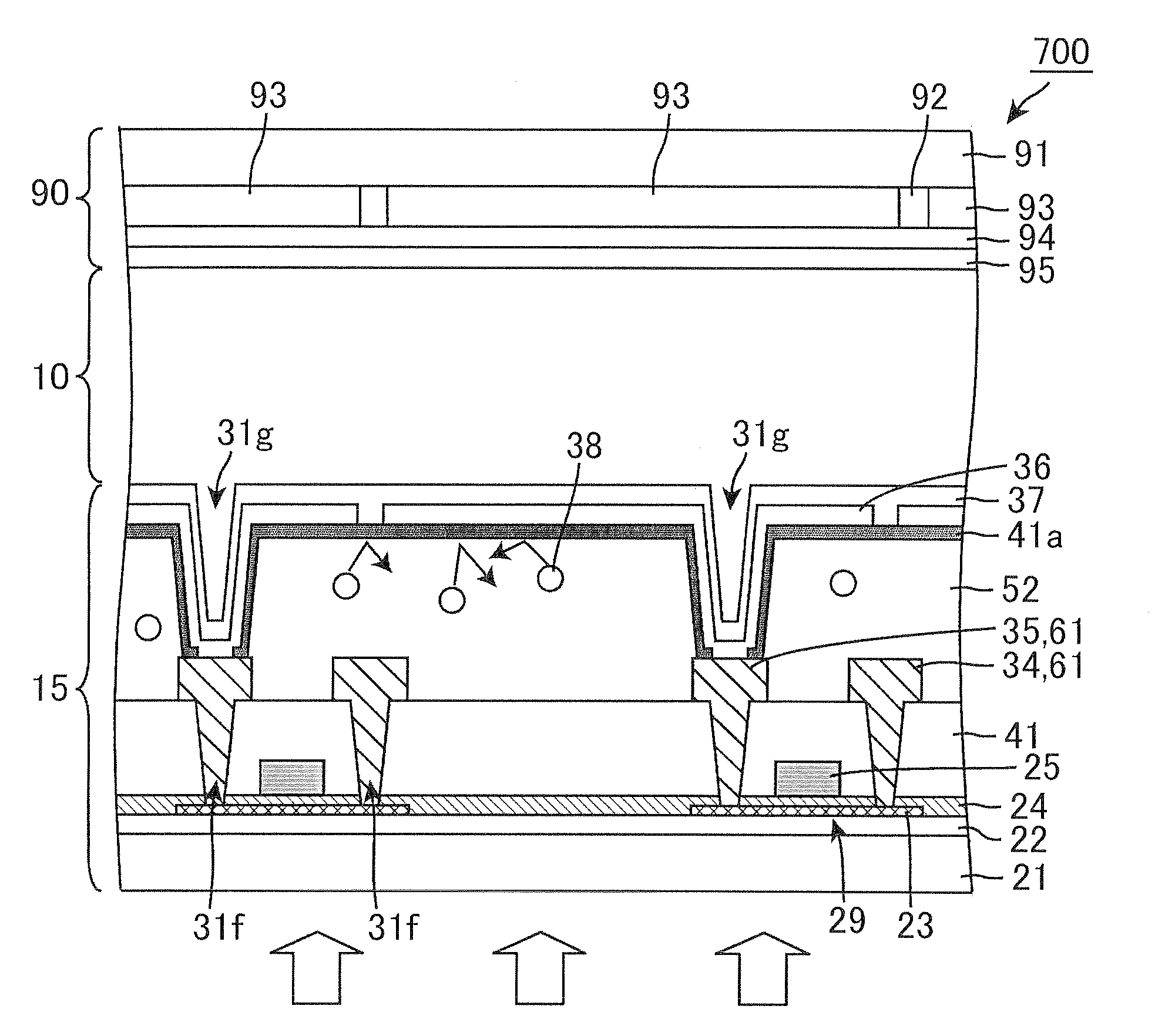
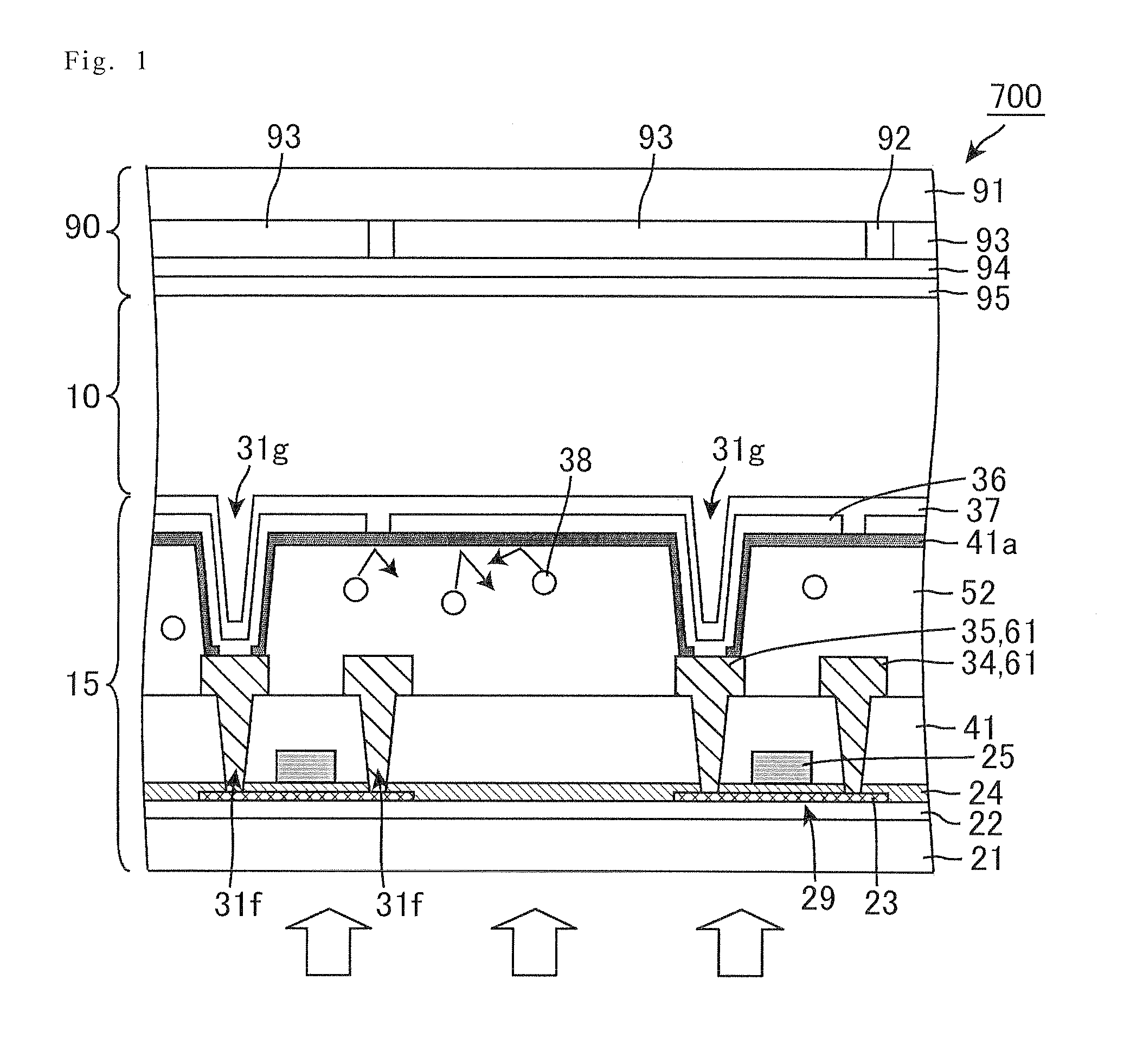
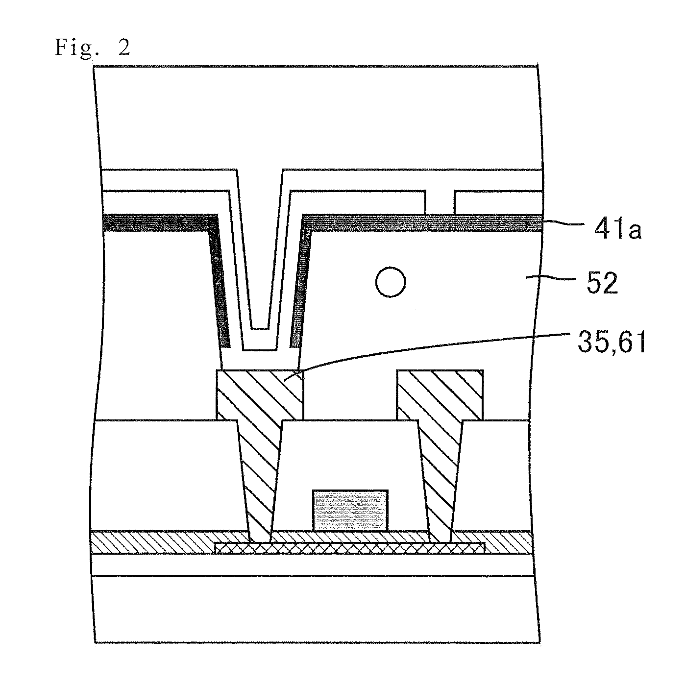
[0109]FIG. 1 is a cross-sectional schematic diagram of a pixel region in a liquid crystal display device of Embodiment 1. A liquid crystal display device 700 of the present Embodiment is a transmissive-type liquid crystal display device, and, as illustrated in FIGS. 1, 37, has a TFT substrate 15 as a display device substrate, and a CF substrate 90 disposed facing the TFT substrate 15. A liquid crystal layer 10 is formed by sealing a liquid crystal material between the two substrates 15, 90 by way of a sealing material 39 provided at the periphery of the substrates 15, 90.

[0110]The TFT substrate 15 has a structure wherein an insulating substrate 21 at a pixel region (display region at which a plurality of pixels is arranged) has sequentially stacked thereon, from the side of the insulating substrate 21, a base coat film 22, a semiconductor layer 23, a gate insulator 24, a gate electrode 25, an inorganic insulating film 41 functioning as an interlayer insulating film, a source electro...

embodiment 2

[0166]FIG. 4 is a cross-sectional schematic diagram of a pixel region in an organic EL display of Embodiment 2. Recurrent features common to the present Embodiment and Embodiment 1 will not be explained again.

[0167]An organic EL display 800 of the present Embodiment is an active matrix-type organic EL display, and has a TFT substrate 16 as a display device substrate, and a sealing substrate 72 disposed facing the TFT substrate 16, as illustrated in FIG. 4.

[0168]Like the TFT substrate 15 of Embodiment 1, the TFT substrate 16 has a structure wherein, at a pixel region, an insulating substrate 21 has sequentially stacked thereon, from the side of the insulating substrate 21, a base coat film 22, a semiconductor layer 23, a gate insulator 24, a gate electrode 25, an inorganic insulating film 41 functioning as an interlayer insulating film, a source electrode 34 and drain electrode 35 comprising a first wiring layer 61, and a stack of a photosensitive resin film 52 and an inorganic insul...

embodiment 3

[0194]FIG. 5 is a cross-sectional schematic diagram of a frame region in a liquid crystal display device of Embodiment 3, wherein FIG. 5(a) illustrates a terminal area, and FIG. 5(b) illustrates a peripheral circuit region. FIG. 6 is a cross-sectional schematic diagram of a pixel region in a liquid crystal display device of Embodiment 3. As illustrated in FIG. 5(a), a liquid crystal display device 100 of the present Embodiment has a structure wherein a TFT substrate 11, being a display device substrate, and an FPC board 70, being another circuit board, are connected by way of an ACF 80, at a terminal area.

[0195]The liquid crystal display device 100 is formed by stacking, on an insulating substrate, a black matrix comprising a light-shielding member; red, green and blue color filters; an overcoat layer; a common electrode comprising a transparent conductive film; and an alignment film, in this order from the insulating substrate. The liquid crystal display device 100 has also a CF su...


PUM

PropertyMeasurementUnit
temperatureaaaaaaaaaa
heightaaaaaaaaaa
heightaaaaaaaaaa

Abstract

The present invention provides a display device substrate, a display device substrate manufacturing method, a display device, a liquid crystal display device, a liquid crystal display device manufacturing method and an organic electroluminescent display device that allow suppressing faults derived from occurrence of gas and/or bubbles in a pixel region. The present invention is a display device substrate that comprises: a photosensitive resin film; and a pixel electrode, in this order, from a side of an insulating substrate. The display device substrate has a gas-barrier insulating film, at a layer higher than the photosensitive resin film, for preventing advance of a gas generated from the photosensitive resin film, or has a gas-barrier insulating film, between the photosensitive resin film and the pixel electrode, for preventing advance of gas generated from the photosensitive resin film.

Description

TECHNICAL FIELD[0001]The present invention relates to a display device substrate, a display device substrate manufacturing method, a display device, a liquid crystal display device, a liquid crystal display device manufacturing method and an organic electroluminescent display device. More specifically, the present invention relates to a display device substrate, a display device substrate manufacturing method, a display device, a liquid crystal display device, a liquid crystal display device manufacturing method and an organic electroluminescent display device that are suitable for a liquid crystal display device or an organic EL display wherein a photosensitive resin film is provided on a substrate.BACKGROUND ART[0002]Multi-domain vertical alignment (MVA) is a known mode among display modes in liquid crystal display devices. In MVA mode liquid crystal display devices, there is used a liquid crystal having negative dielectric constant anisotropy, sealed between a pair of substrates,...

Claims


Application Information

Patent Timeline
Patent Type & Authority Applications(United States)
IPC IPC(8): G02F1/1333H01J40/16B29D11/00G03F7/20
CPCG02F1/136227G02F2201/50H01L51/5203H01L51/5237G02F1/133345H01L27/3258G02F2201/501H10K59/124H10K50/8445H10K50/841H10K50/805H10K50/11H10K50/81H10K50/8426H10K59/122H10K59/131H10K50/84H10K2102/00
Inventor MORIWAKI, HIROYUKI
Owner SHARP KK
Why Eureka
Try Eureka