Monolithic integration of silicon and group III-V devices

a semiconductor and monolithic technology, applied in the field of monolithic integration of silicon and group iii-v semiconductor device fabrication, can solve the problems of increasing the area consumed on the pc, increasing the parasitic inductance, capacitance and resistance, and often not being compatible with popular and commonly used silicon devices

Active Publication Date: 2011-09-01
INFINEON TECH AMERICAS CORP
View PDF103 Cites 79 Cited by
  • Summary
  • Abstract
  • Description
  • Claims
  • Application Information

AI Technical Summary

Benefits of technology

[0009]The present invention is directed to monolithic integration of silicon and group III-V semiconductor devices, substantial

Problems solved by technology

However, the fabrication of group III-V devices, such as, GaN transistors, is often not compatible with popular and commonly used silicon devices.
The separate dies increase fabrication cost, packaging cost, area consumed on a PC board, and result in increase

Method used


Image

  • Monolithic integration of silicon and group III-V devices
  • Monolithic integration of silicon and group III-V devices
  • Monolithic integration of silicon and group III-V devices

Examples


Embodiment Construction

[0016]The present invention is directed to monolithic integration of silicon and group III-V semiconductor devices. The following description contains specific information pertaining to the implementation of the present invention. One skilled in the art will recognize that the present invention may be implemented in a manner different from that specifically discussed in the present application. Moreover, some of the specific details of the invention are not discussed in order not to obscure the invention.

[0017]The drawings in the present application and their accompanying detailed description are directed to merely exemplary embodiments of the invention. To maintain brevity, other embodiments of the present invention are not specifically described in the present application and are not specifically illustrated by the present drawings.

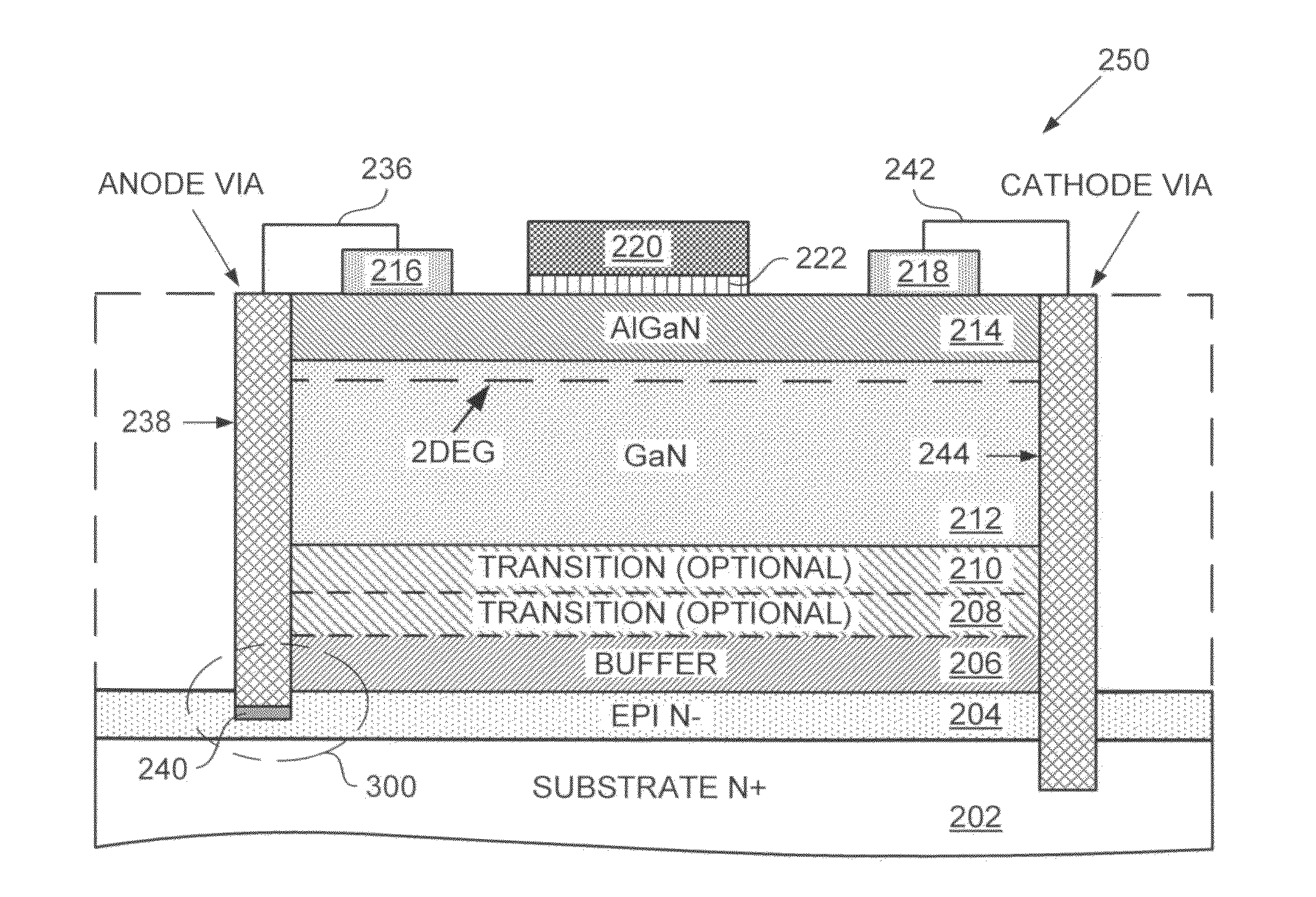
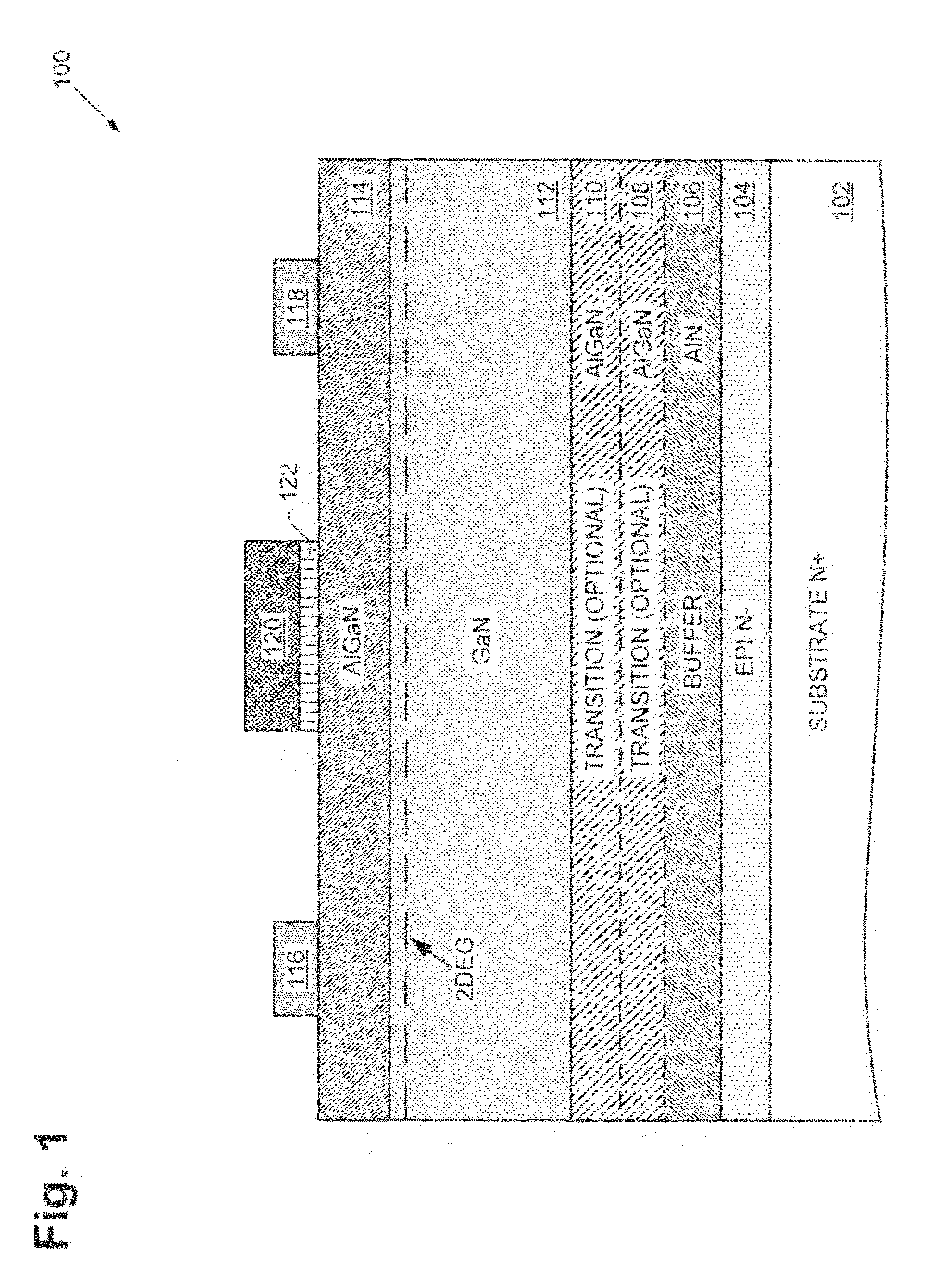
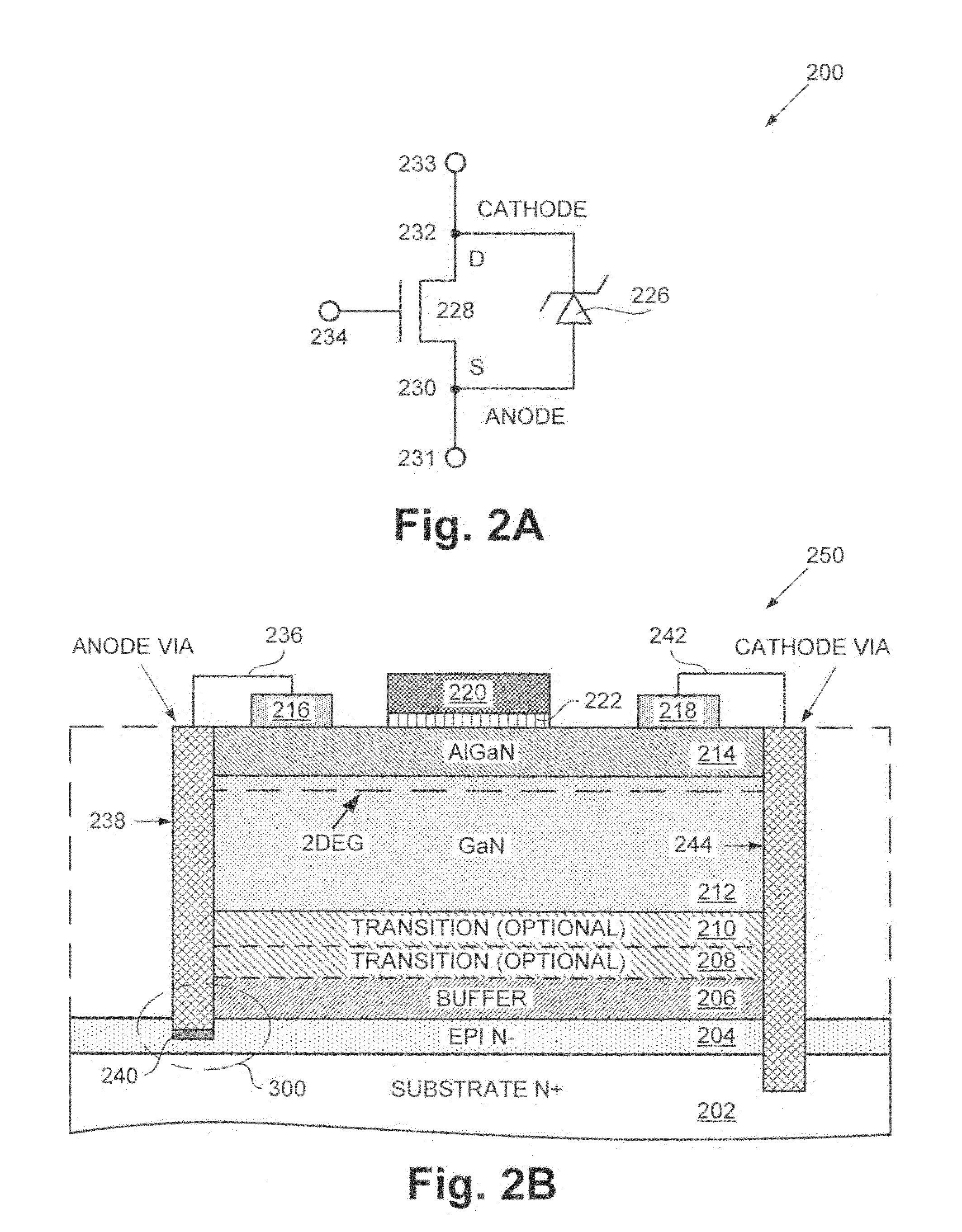
[0018]FIG. 1 shows a cross-sectional view of exemplary group III-V semiconductor device 100, and more particularly shows a III-Nitride high electron mo...


PUM


Abstract

Disclosed is a monolithically integrated silicon and group III-V device that includes a group III-V transistor formed in a III-V semiconductor body disposed over a silicon substrate. At least one via extends through the III-V semiconductor body to couple at least one terminal of the group III-V transistor to a silicon device formed in the silicon substrate. The silicon device can be a Schottky diode, and the group III-V transistor can be a GaN HEMT. In one embodiment an anode of the Schottky diode is formed in the silicon substrate. In another embodiment, the anode of the Schottky diode is formed in a lightly doped epitaxial silicon layer atop the silicon substrate. In one embodiment a parallel combination of the Schottky diode and the group III-V transistor is formed, while in another embodiment is series combination is formed.

Description

[0001]The present application claims the benefit of and priority to a pending provisional application entitled “Monolithic Integration of Silicon and Group III-V Devices and Efficient Circuits Utilizing Same,” Ser. No. 61 / 339,190 filed on Mar. 1, 2010. The disclosure in that pending provisional application is hereby incorporated fully by reference into the present application.DEFINITION[0002]In the present application, “group semiconductor” or “group III-V device” or similar terms refers to a compound semiconductor that includes at least one group III element and at least one group V element, such as, but not limited to, gallium nitride (GaN), gallium arsenide (GaAs), indium aluminum gallium nitride (InAlGaN), indium gallium nitride (InGaN) and the like. Analogously, “III-nitride semiconductor” refers to a compound semiconductor that includes nitrogen and at least one group III element, such as, but not limited to, GaN, AlGaN, InN, AlN, InGaN, InAlGaN and the like.BACKGROUND OF THE ...

Claims


Application Information

Patent Timeline
IPC IPC(8): H01L27/06
CPCH01L21/8258H01L27/0629H03K17/567H01L27/0688H01L29/7786H01L29/2003H03K17/74
Inventor BRIERE, MICHAEL A.
Owner INFINEON TECH AMERICAS CORP
Why Eureka
Try Eureka