Method for manufacturing semiconductor device

a manufacturing method and semiconductor technology, applied in the direction of semiconductor devices, basic electric elements, electrical appliances, etc., can solve the problems of increasing the power consumption of the semiconductor device, and achieve the effects of reducing the impurities left in the oxide semiconductor layer, high reliability of the semiconductor device, and suppressing the variation of threshold voltag

Active Publication Date: 2011-09-01
SEMICON ENERGY LAB CO LTD
View PDF99 Cites 52 Cited by
  • Summary
  • Abstract
  • Description
  • Claims
  • Application Information

AI Technical Summary

Benefits of technology

[0008]In a transistor which utilizes semiconductor characteristics, it is preferable that variation in threshold voltage caused by time degradation be small and the off-state current be small. For example, when a transistor whose threshold voltage varies greatly owing to time degradation is used for a semiconductor device, the reliability of the semiconductor device is lowered. In addition, when a transistor whose off-state current is large is used for a semiconductor device, the power consumption of the semiconductor device is increased.

Problems solved by technology

In addition, when a transistor whose off-state current is large is used for a semiconductor device, the power consumption of the semiconductor device is increased.

Method used


Image

  • Method for manufacturing semiconductor device
  • Method for manufacturing semiconductor device
  • Method for manufacturing semiconductor device

Examples


embodiment 1

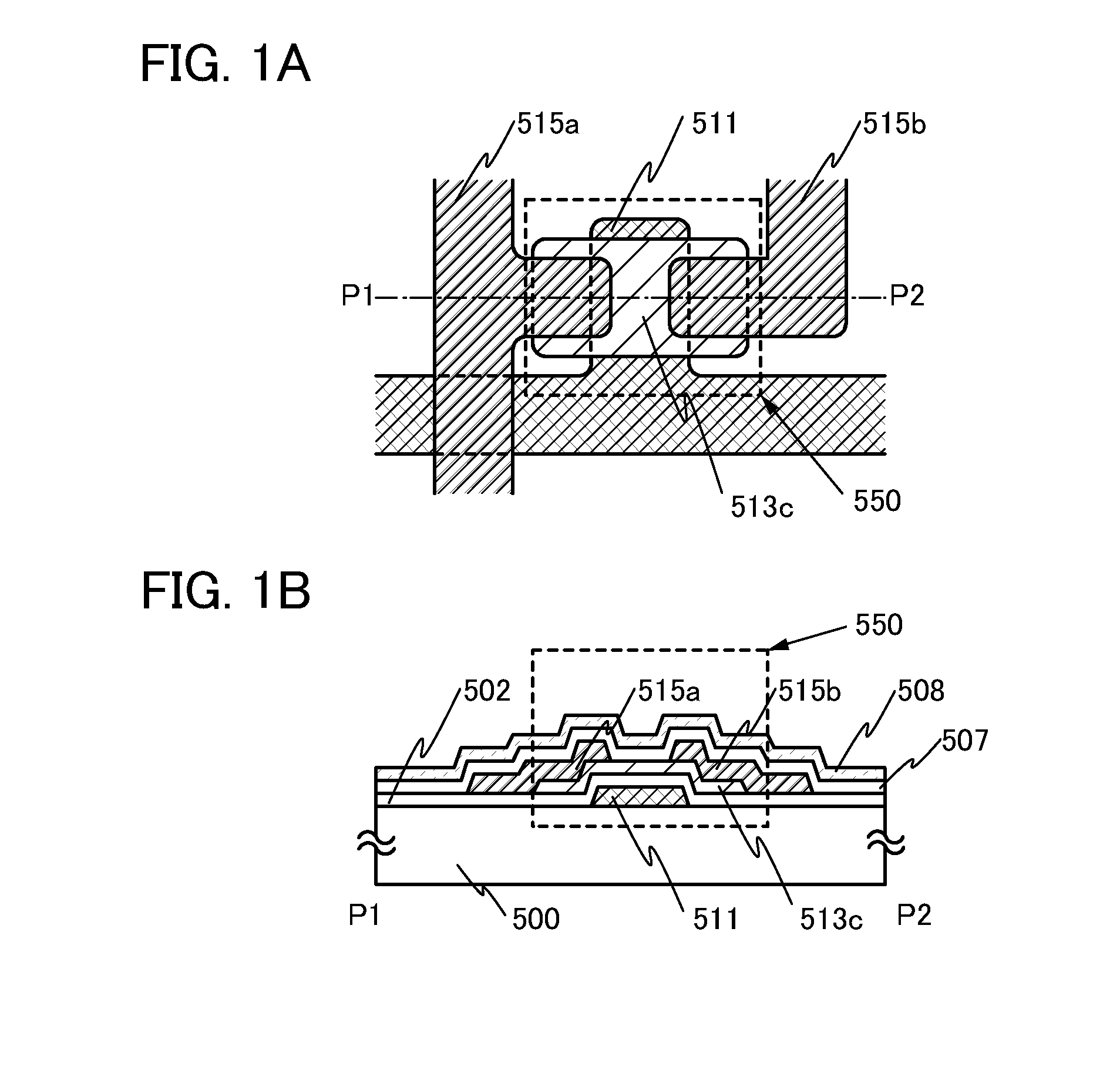
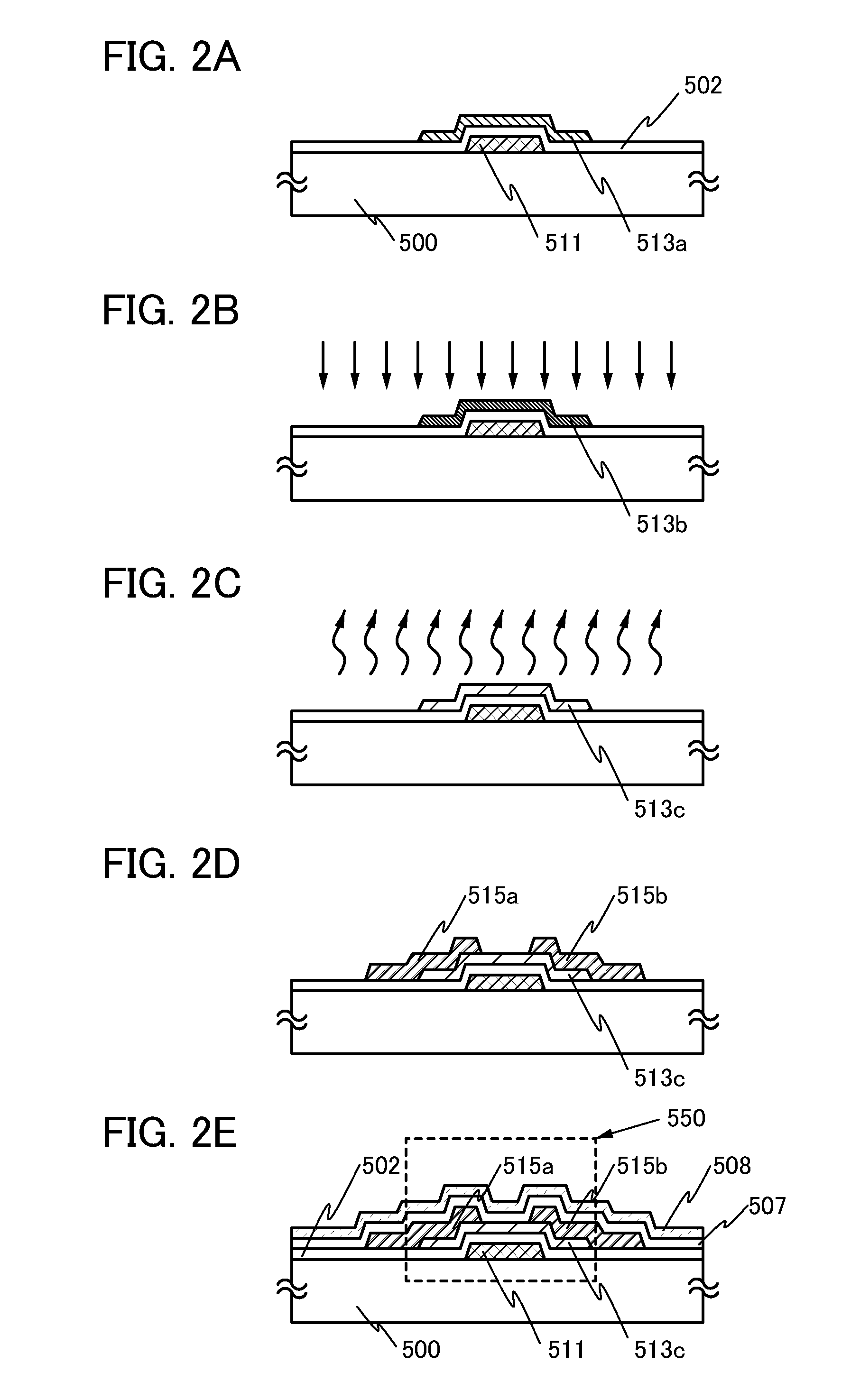
[0051]In this embodiment, a method for manufacturing a bottom-gate transistor will be described with reference to FIGS. 1A and 1B and FIGS. 2A to 2E. In the method, after oxygen is added to an oxide semiconductor layer, heat treatment is performed on the oxide semiconductor layer so as to remove impurities and highly purify the oxide semiconductor layer.

[0052]FIGS. 1A and 1B illustrate a structure of a transistor 550 that is bottom-gate type manufactured in this embodiment. FIG. 1A is a top view of the transistor 550 and FIG. 1B is a cross-sectional view of the transistor 550. FIG. 1B illustrates a cross section along line P1-P2 in FIG. 1A.

[0053]In the transistor 550, a gate electrode 511 and a gate insulating layer 502 which covers the gate electrode 511 are provided over a substrate 500 having an insulating surface. An oxide semiconductor layer 513c which is highly purified and overlaps with the gate electrode 511 is provided over the gate insulating layer 502. In addition, a firs...

embodiment 2

[0112]In this embodiment, a method for manufacturing a top-gate transistor will be described with reference to FIGS. 3A and 3B and FIGS. 4A to 4E. In the method, a method in which an oxide semiconductor layer is highly purified by performing heat treatment on the oxide semiconductor layer after addition of oxygen to remove impurities is used.

[0113]FIGS. 3A and 3B illustrate a structure of a transistor 650 that is a top-gate type manufactured in this embodiment. FIG. 3A is a top view of the transistor 650 and FIG. 3B is a cross-sectional view of the transistor 650. FIG. 3B illustrates a cross section along line Q1-Q2 in FIG. 3A.

[0114]In the transistor 650, over a substrate 600 having an insulating surface, a first electrode 615a and a second electrode 615b which serve as a source electrode and a drain electrode are provided. An oxide semiconductor layer 613c which is highly purified and covers end portions of the first electrode 615a and the second electrode 615b, and a gate insulati...

embodiment 3

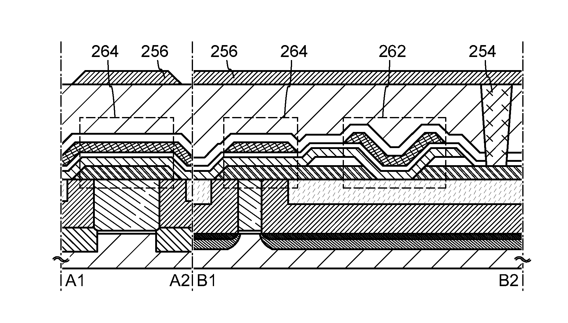
[0148]In this embodiment, a structure and a manufacturing method of a semiconductor device according to an embodiment of the present invention will be described with reference to FIGS. 5A and 5B, FIGS. 6A to 6D, FIGS. 7A to 7C, FIGS. 8A to 8D, and FIGS. 9A to 9C. The semiconductor device described in this embodiment can be used as a memory device.

[0149]FIGS. 5A and 5B illustrate the structure of the semiconductor device described in this embodiment. FIG. 5A is a cross-sectional view of the semiconductor device, and FIG. 5B is a top view of the semiconductor device. Note that FIG. 5A corresponds to a cross section along line A1-A2 and line B1-B2 in FIG. 5B.

[0150]The semiconductor device described in this embodiment includes a transistor 260 formed using a first semiconductor material in a lower portion, a transistor 262 formed using a second semiconductor material in an upper portion, and a capacitor 264. A gate electrode 210 of the transistor 260 is directly connected to a first ele...


PUM


Abstract

It is an object to provide a highly reliable semiconductor device, a semiconductor device with low power consumption, a semiconductor device with high productivity, and a method for manufacturing such a semiconductor device. Impurities left remaining in an oxide semiconductor layer are removed without generating oxygen deficiency, and the oxide semiconductor layer is purified to have an extremely high purity. Specifically, after oxygen is added to the oxide semiconductor layer, heat treatment is performed on the oxide semiconductor layer to remove the impurities. In order to add oxygen, it is preferable to use a method in which oxygen having high energy is added by an ion implantation method, an ion doping method, or the like.

Description

TECHNICAL FIELD[0001]The present invention relates to a method for manufacturing a semiconductor device including an oxide semiconductor. In this specification, a semiconductor device generally refers to an element or a device which functions by utilizing semiconductor characteristics.BACKGROUND ART[0002]A technique in which a transistor is formed using a semiconductor layer formed over a substrate having an insulating surface is known. For example, a technique in which a transistor is formed over a glass substrate using a thin film containing a silicon-based semiconductor material and applied to a liquid crystal display device and the like is known.[0003]A transistor used for a liquid crystal display device is mainly formed using a semiconductor material such as amorphous silicon or polycrystalline silicon. Although a transistor formed using amorphous silicon has low field-effect mobility, it can be formed over a larger glass substrate. Meanwhile, a transistor formed using polycrys...

Claims


Application Information

Patent Timeline
Patent Type & Authority Applications(United States)
IPC IPC(8): H01L21/336
CPCH01L27/1225H01L29/66742H01L21/02521H01L29/7869H01L21/02554H01L21/02565H01L21/324H01L21/425
Inventor YAMAZAKI, SHUNPEIOHARA, HIROKI
Owner SEMICON ENERGY LAB CO LTD
Why Eureka
Try Eureka