Method, system, and program product for interactive checking for double pattern lithography violations

a technology of double pattern lithography and interactive testing, applied in the field of electronic design automation, can solve the problems of inability to project an accurate image of increasingly smaller features onto the wafer, conventional tools do not have the ability to interactively track, and non-standard geometries on a single layer normally cannot be printed on silicon

Active Publication Date: 2011-09-08
CADENCE DESIGN SYST INC
View PDF17 Cites 50 Cited by
  • Summary
  • Abstract
  • Description
  • Claims
  • Application Information

AI Technical Summary

Problems solved by technology

However, the ability to project an accurate image of increasingly smaller features onto the wafer is limited by the wavelength of the light used, and the ability of the lens system.
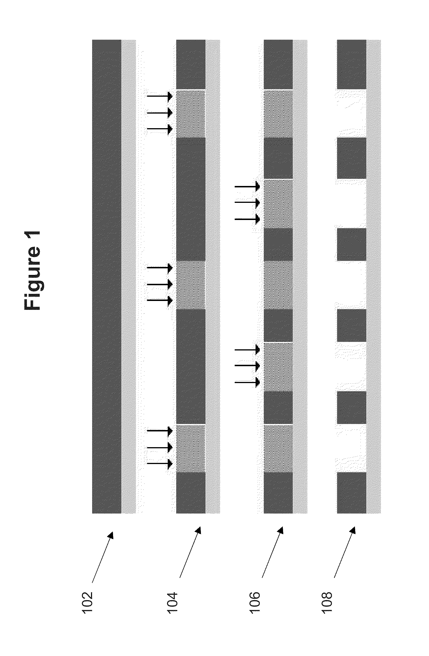
For deep sub-micron semiconductor manufacturing process, such as processes at feature sizes of 22 nm and below, the layout geometries on a single layer normally cannot be printed on silicon with a single lithography mask except with great difficulty and / or manufacturing defects / problems.
While this new technology theoretically may be used to manufacture semiconductor devices, EDA tools do not yet exist which can be used to interactively design and check double patterning designs.
For example, conventional tools do not have the ability to interactively track the division of a single layer of the design into multiple masks / patterns for double patterning, and to interactively check the feasibility of mask making for lithography purposes during layout editing.
However, this batch-based approach requires the layout editor to finish the creation of all necessary geometries before it can know of the possible violations for mask making.
Therefore, the batch-based approach is not efficient for layout creation when the layout is interactively created / modified by manual editing.

Method used


Image

  • Method, system, and program product for interactive checking for double pattern lithography violations
  • Method, system, and program product for interactive checking for double pattern lithography violations
  • Method, system, and program product for interactive checking for double pattern lithography violations

Examples


Embodiment Construction

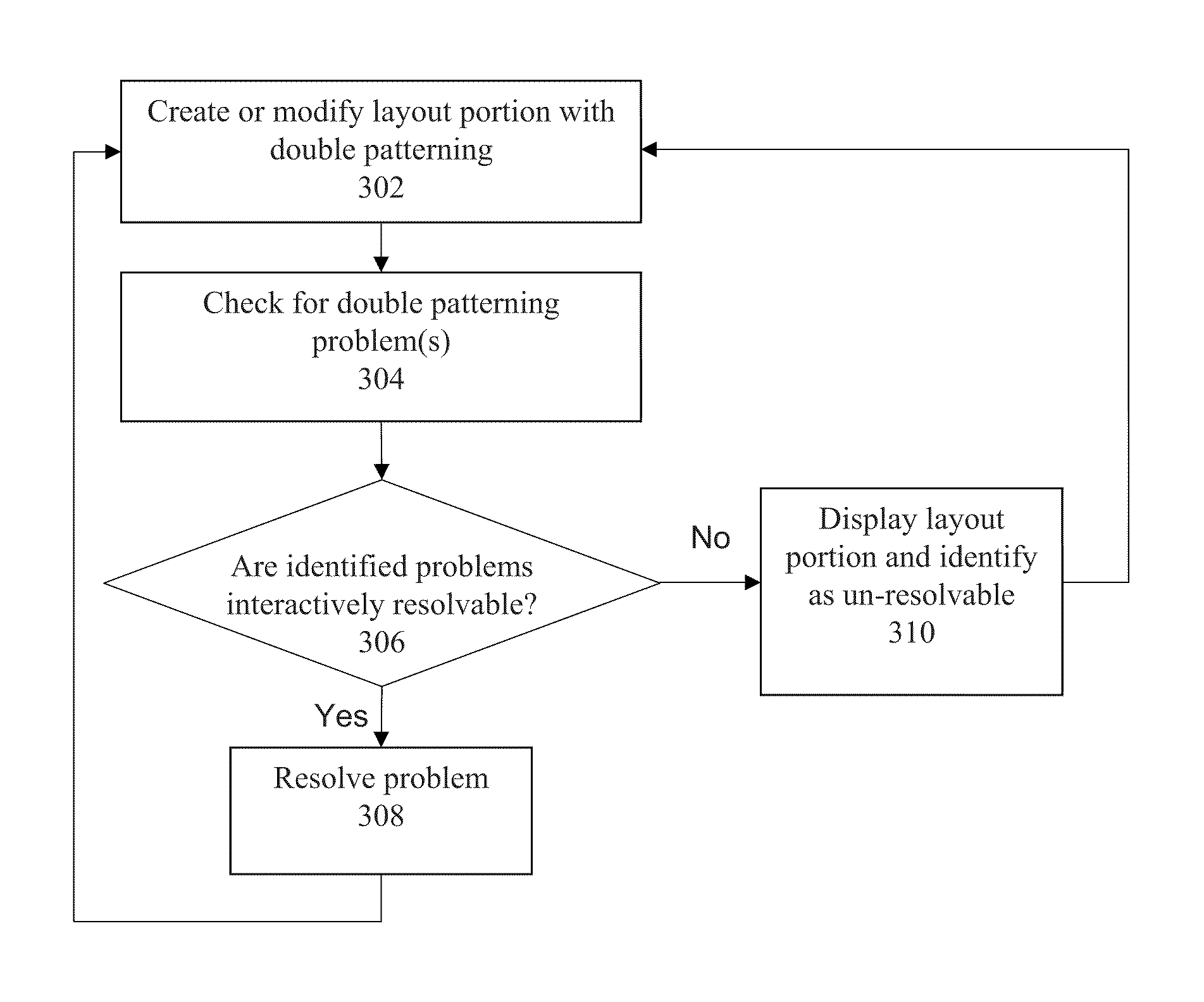
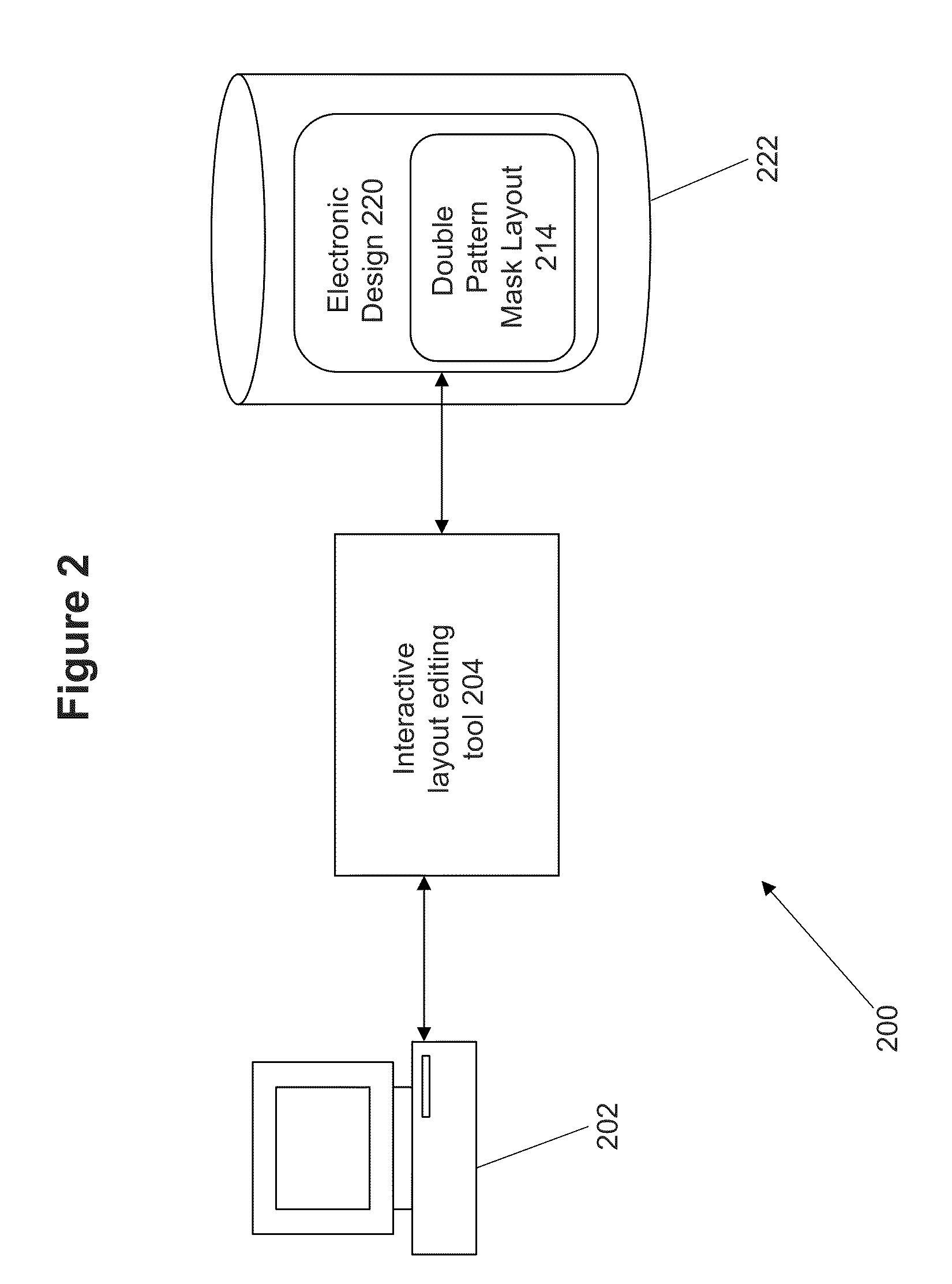
[0022]Embodiments of the present invention provide a method, apparatus, and program product for performing interactive layout editing to address double patterning approaches to implement lithography of electronic designs. A feature of an embodiment of the present invention is to perform spatial query around the shape(s) being created during editing with the distance of allowed spacing in a single mask. If a design error is encountered, corrective editing may occur to correct the error. The present approach can be configured to allow the error detection and corrective actions to be performed interactively.

[0023]To explain the problem being addressed by embodiments of the invention, consider that the minimum feature size that a projection system can print can be expressed by:

CD=k1λNA

where CD, critical dimension, is the minimum feature size; k1 is a dimensionless coefficient of process-related factors; A is the wavelength of light used; and NA is the numerical aperture of the projectio...


PUM


Abstract

Disclosed are a method, apparatus, and computer program product for performing interactive layout editing to address double patterning approaches to implement lithography of electronic designs. A spatial query is performed around the shape(s) being created during editing with the distance of allowed spacing in a single mask. If a design error is encountered, corrective editing may occur to correct the error. Checking may occur to make sure that the error detection and corrective actions can be performed interactively.

Description

TECHNICAL FIELD[0001]This invention concerns electronic design automation for performing interactive checking of electronic designs with regard to double pattern lithography violations.DESCRIPTION OF THE RELATED ART[0002]Integrated circuits, or ICs, are created by patterning a substrate and materials deposited on the substrate. The substrate is typically a semiconductor wafer. The patterned features make up devices and interconnections. This process generally starts with a designer creating an integrated circuit by hierarchically defining functional components of the circuit using a hardware description language. From this high-level functional description, a physical circuit implementation dataset is created, which is usually in the form of a netlist. This netlist identifies logic cell instances from a cell library, and describes cell-to-cell connectivity.[0003]A layout file is then created using the netlist. This is accomplished through a placing and routing process, which assigns...

Claims


Application Information

Patent Timeline
Patent Type & Authority Applications(United States)
IPC IPC(8): G06F17/50
CPCG06F17/50G06F30/00G06F30/398G03F1/70G03F1/36G06F2119/18G06F30/39
Inventor CAO, MINRUEHL, ROLAND
Owner CADENCE DESIGN SYST INC
Why Eureka
Try Eureka