
Integrated circuit package for semiconductior devices with improved electric resistance and inductance

Active Publication Date: 2011-09-15
ALPHA & OMEGA SEMICON INC
View PDF4 Cites 23 Cited by
  • Summary
  • Abstract
  • Description
  • Claims
  • Application Information

AI Technical Summary

Benefits of technology

[0012]The preferred embodiment of the integrated circuit package of the present invention solves the aforementioned problems in a straight forward and simple manner.
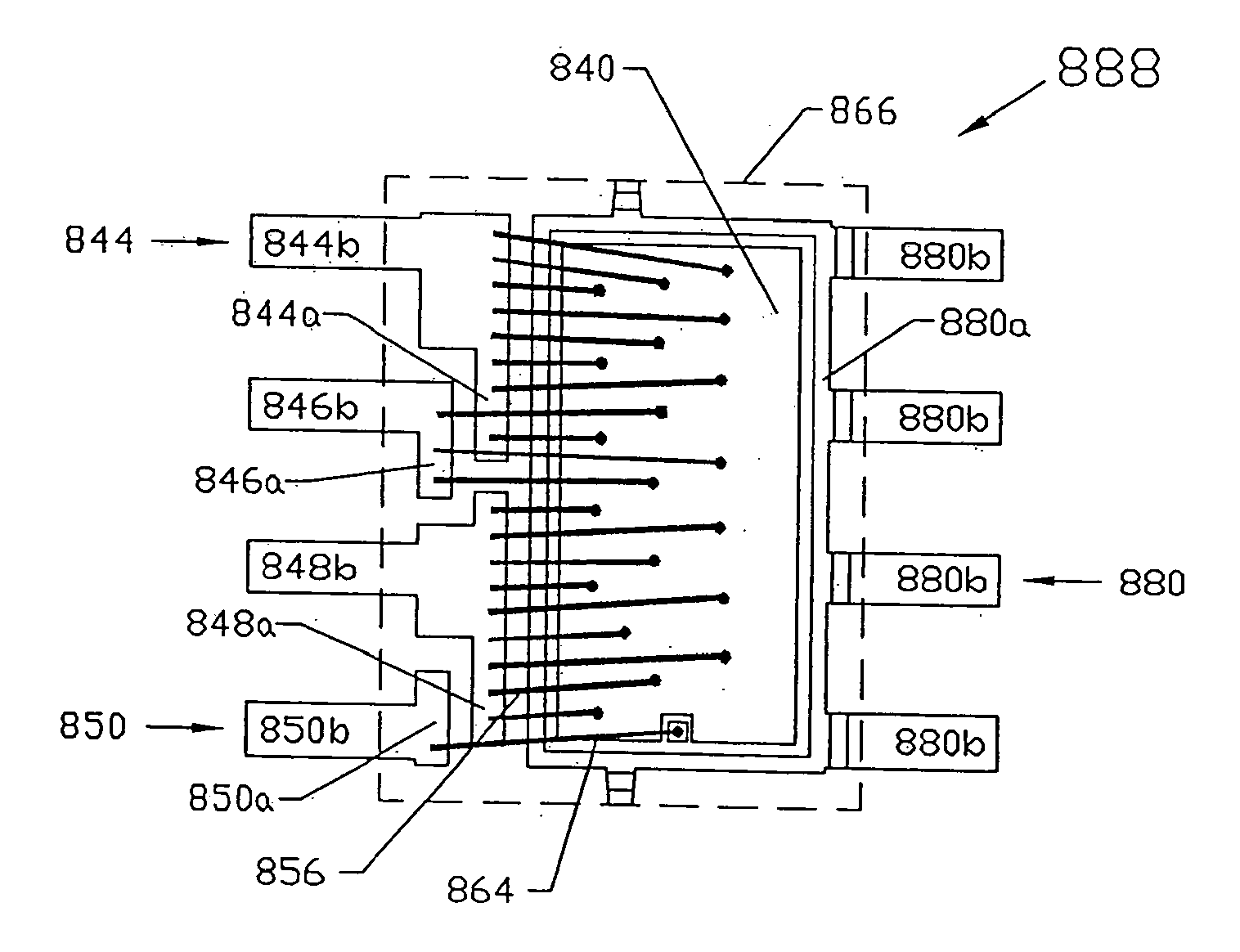
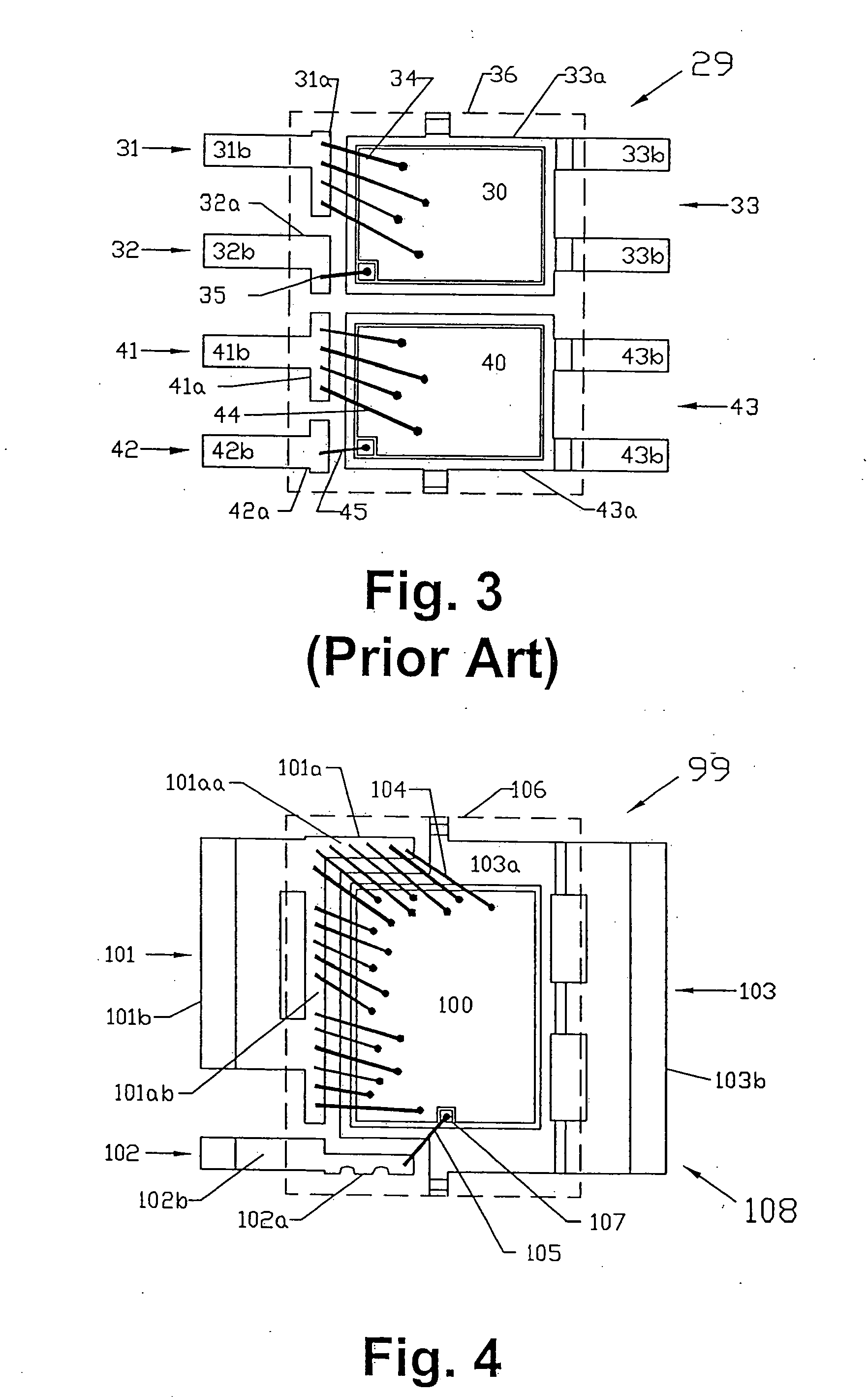
[0013]Broadly, the present invention contemplates a method of improving the package by giving up some of the real estate reserved for the silicon or die to re-distribute a bonding area, such as for the source or other heavy current loaded terminal, about corners and adjacent sides of the die so as to increase the interconnections between such bonding area and the top conductive surface of the die in order to reduce the electrical resistance and inductance.
[0015]Furthermore, the present invention contemplates a method of increasing the surface area of the source and drain terminal areas that are external to the body to dissipate heat quicker and reduce the external terminal resistances. In other words, the area of the leadframe metallization is increased to improve the thermal resistance of the package. This includes fusing all or some of the leads of a terminal, either completely or partially.

Problems solved by technology

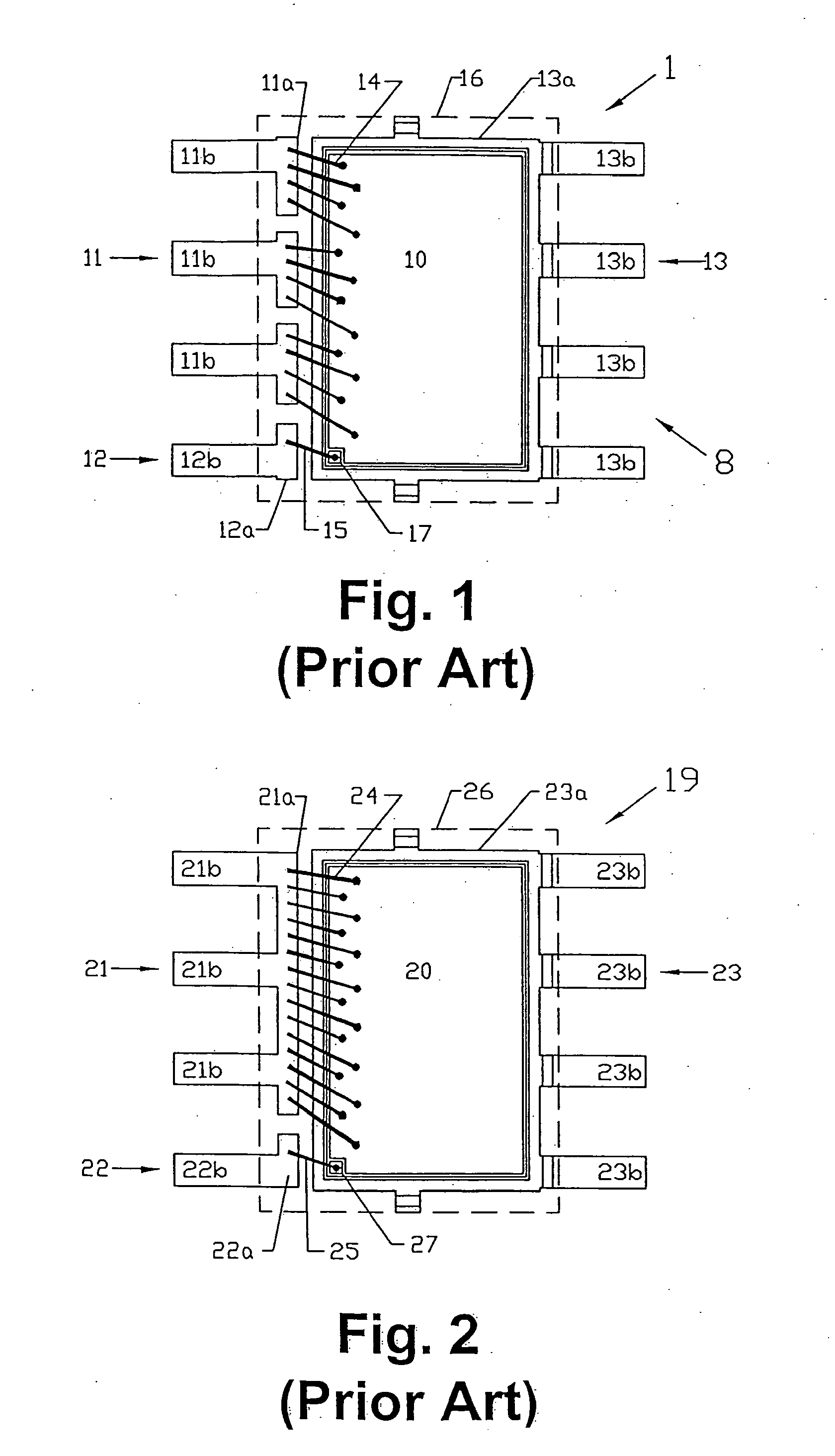
In many cases, package resistance can be equal to the Silicon resistance—this is a very uneconomical use of the device Silicon.
This problem becomes more severe as lower device resistances and improved technology allow for higher operating currents for the same package size.
Furthermore, increasing the surface area of the external source and drain leads, exposed to air, reduces external terminal resistance and allows heat to be dissipated quicker.

Method used


Image

  • Integrated circuit package for semiconductior devices with improved electric resistance and inductance
  • Integrated circuit package for semiconductior devices with improved electric resistance and inductance
  • Integrated circuit package for semiconductior devices with improved electric resistance and inductance

Examples


Embodiment Construction

[0037]Referring now to the drawings and more particularly to FIG. 4, the semiconductor integrated circuit (IC) package of the present invention will be referenced by the numeral 99. The semiconductor integrated circuit (IC) package 99 includes, in general, a semiconductor die 100 disposed over a leadframe pad 103a both of which are molded in a plastic body 106. The package 99 further includes the necessary interconnections well known in the art for coupling the die 100 to the leadframe pad 103a and / or leadframe 108, some of which are described in detail below.

[0038]As will be seen based on the description provided below, the objectives of the present invention can be related to a variety of semiconductor devices. Accordingly, to describe each and every device application is prohibitive. For exemplary purposes, FIG. 4 illustrates a top view of the semiconductor IC package 99 for a MOSFET device having three terminals (e.g. a source terminal 101, a gate terminal 102 and a drain termin...


PUM


Abstract

A semiconductor integrated circuit package having a leadframe (108) that includes a leadframe pad (103a) disposed under a die (100) and a bonding metal area (101a) that is disposed over at least two adjacent sides of the die. The increase in the s bonding metal area (101a) increases the number of interconnections between the metal area (101a) and the die (100) to reduce the electric resistance and inductance. Furthermore, the surface area of the external terminals radiating from the package's plastic body (106) is increased if not maximized so that heat can be dissipated quicker and external terminal, resistances reduced. The integrated circuit is applicable for MOSFET devices and the bonding metal area (101a) is used for the source terminal (101). The bonding metal area may have a “L” shape, a “C” shape, a “J” shape, an “I” shape or any combination thereof.

Description

FIELD OF INVENTION[0001]The present invention is directed to integrated circuit packaging, and more particularly to an integrated circuit (IC) package for power semiconductor devices, such as metal-oxide semiconductor field-effect transistor (MOSFET) devices, that reduces the package electrical resistance, inductance and thermal resistance to enable the device be more efficient and dissipate more power.BACKGROUND OF THE INVENTION[0002]Today's advanced silicon technology allows for very low on-resistance power MOSFETs, enabling the use of small chips operating at very high power densities. In many cases, package resistance can be equal to the Silicon resistance—this is a very uneconomical use of the device Silicon. There is constant thrust to lower cost by decreasing package resistance. Due to the higher power densities, there is a need to have packages with lower thermal resistance. Package parasitic inductance can contribute to a majority of the power dissipated in the MOSFET in hi...

Claims


Application Information

Patent Timeline
IPC IPC(8): H01L27/092H01L21/60H01L23/485H01L23/495H01L23/50
CPCH01L23/4952H01L2924/1306H01L23/49575H01L23/50H01L24/05H01L24/06H01L24/48H01L24/49H01L24/85H01L2224/04042H01L2224/05599H01L2224/05647H01L2224/0603H01L2224/48137H01L2224/48247H01L2224/48465H01L2224/4903H01L2224/49051H01L2224/49111H01L2224/49171H01L2224/49431H01L2224/85447H01L2924/01002H01L2924/01005H01L2924/01006H01L2924/01014H01L2924/01029H01L2924/01047H01L2924/01075H01L2924/01082H01L2924/13091H01L2924/14H01L2924/19041H01L2924/19043H01L2924/30107H01L23/49562H01L2924/01033H01L2924/00014H01L2224/45099H01L2924/00H01L2924/00012H01L2924/181
Inventor LUO, LEESHAWNBHALLA, ANUPHO, YUEH-SELUI, SIK K.CHANG, MIKE
Owner ALPHA & OMEGA SEMICON INC
Learn More