Piezoelectric element, piezoelectric sensor, electronic device, and method for manufacturing piezoelectric element

a piezoelectric element and piezoelectric sensor technology, applied in the direction of device material selection, generator/motor, mechanical vibration separation, etc., can solve the problems of reduced sound pressure of ultrasound output, increased electrical resistance, and difficulty in controlling in high-frequency regions, so as to inhibit any increase in electrical resistance and simplify manufacturing process

Active Publication Date: 2011-09-15
SEIKO EPSON CORP
View PDF6 Cites 22 Cited by
  • Summary
  • Abstract
  • Description
  • Claims
  • Application Information

AI Technical Summary

Benefits of technology

[0008]In view of the above-mentioned problems, an object of the present invention is to provide a piezoelectric element, a piezoelectric sensor, an electronic device, and a method for manufacturing the piezoelectric element, in which the electrical resistance of an electrode can be reduced.
[0029]As with the aspects of the invention described above, manufacturing the piezoelectric element according to the manufacturing method described above makes it possible to inhibit any increase in the electrical resistance of the lower electrode layer. Also, since it is possible to form the first piezoelectric layer and the second piezoelectric layer at the same time, the manufacturing process can be made simpler compared to a method in which, e.g., a protective film for protecting the lower electrode layer is separately formed.

Problems solved by technology

Thus, when the film thickness dimension of the metal electrode film is reduced, the electrical resistance is increased, and problems are presented in that, for example, electricity consumption is increased, the sound pressure of the ultrasound output is reduced, and control in a high-frequency region becomes difficult.
Although the lower electrode layer may be formed so as to have a large initial thickness dimension in order to account for over-etching of the lower electrode layer as described above, a problem is presented in such an instance in that a portion on which the piezoelectric layer is formed as a layer is not subjected to over-etching, and the thickness dimension of the lower electrode layer is therefore increased, and the total thickness dimension of a portion in which the piezoelectric layer and the upper electrode layer are layered is increased.
In an instance in which a plurality of wiring patterns are formed on the same planar substrate, there is a possibility of the size of the substrate or other factors causing the line width of each of the wiring patterns to be restricted and increasing the electrical resistance.
However, when the piezoelectric element is actually arranged on the substrate, there are instances in which the lower electrode wiring cannot be provided so as to have a sufficient line width, and the line width is smaller than that of the element connection wiring, owing to other elements and their wiring patterns.

Method used


Image

  • Piezoelectric element, piezoelectric sensor, electronic device, and method for manufacturing piezoelectric element
  • Piezoelectric element, piezoelectric sensor, electronic device, and method for manufacturing piezoelectric element
  • Piezoelectric element, piezoelectric sensor, electronic device, and method for manufacturing piezoelectric element

Examples


first embodiment

Operation and Effect of First Embodiment

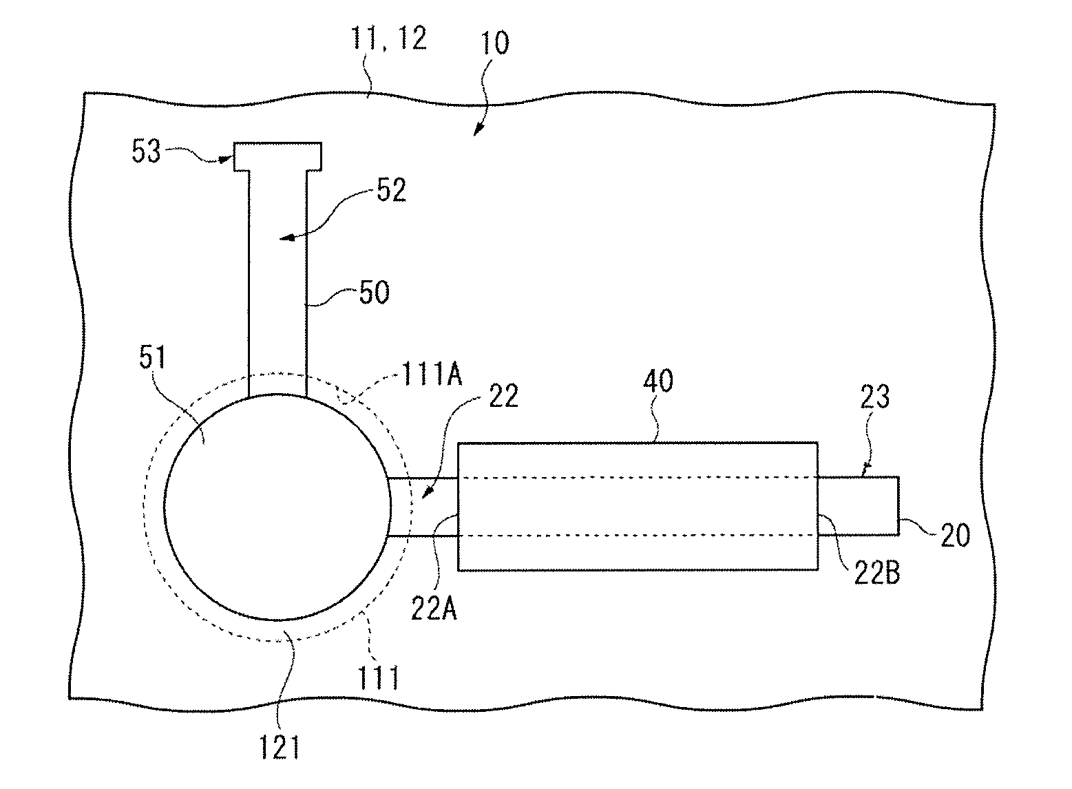
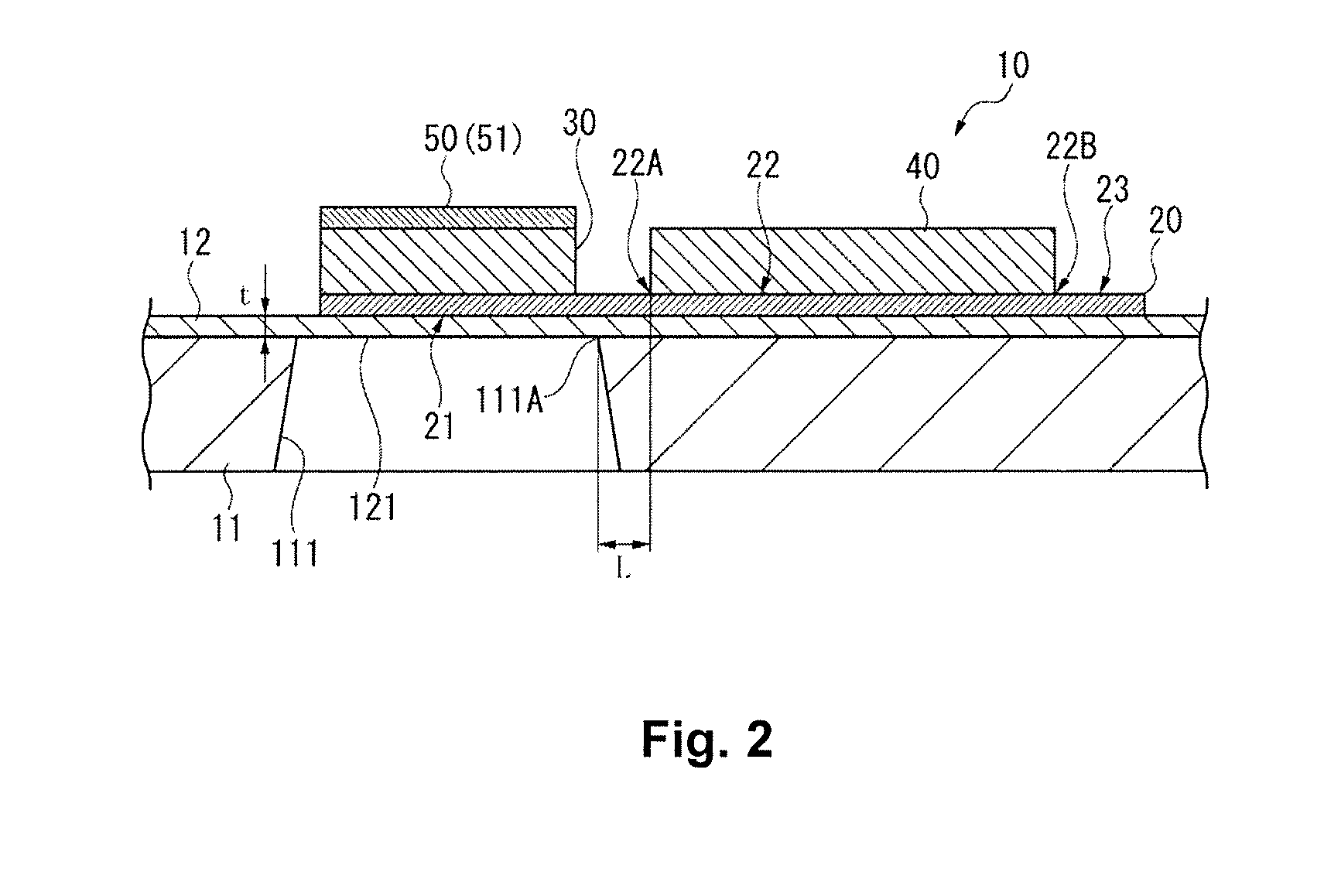
[0076]As described above, in the piezoelectric element according to the first embodiment, the first piezoelectric layer 30 is formed on the lower main electrode body 21, which is a portion of the lower electrode layer 20 formed across the interior and exterior of the opening part 111 that is formed inside the opening part 111, and the second piezoelectric layer 40 is formed on a portion of the lower electrode wire part 22 that is outside the opening part 111.

[0077]Therefore, it is possible to prevent the disadvantage of the lower electrode layer being over-etched and the electrical resistance increasing when etching is performed on the piezoelectric layer 60 and the first piezoelectric layer 30 and the second piezoelectric layer 40 are being formed. Accordingly, the amount of expansion and contraction of the first piezoelectric layer 30 can be increased using a lower electrical power, and the sound pressure of the ultrasound produced by vibrat...

second embodiment

Example of Modification of Second Embodiment

[0094]Although the example of the second embodiment described above shows, as a wiring layer, an auxiliary electrode layer 70 for providing a connection between two points on the lower electrode layer 20 (i.e., between the end part position 22A and the connecting part 22B), the configuration is not limited to that described above. A configuration shown in FIGS. 6, 7, and 8 is also possible.

[0095]FIG. 6 is a plan view of a part of a lower electrode wire part 22 of a piezoelectric element according to an example of a modification of the second embodiment, viewed from the thickness direction of the substrate 11. FIG. 7 is a cross-section view along line A-A in FIG. 6. FIG. 8 is a cross-section view along line B-B in FIG. 6;

[0096]In the piezoelectric element, a second piezoelectric layer 40A having a width dimension that is smaller than that of the lower electrode wire part 22 is provided on the lower electrode wire part 22. Also, as shown in ...

third embodiment

[0098]Next, a piezoelectric element according to a third embodiment of the present invention will now be described with reference to the accompanying drawings.

[0099]FIGS. 9A and 9B are views showing the piezoelectric element according to the third embodiment, where FIG. 9A is a plan view and FIG. 9B is a cross-section view.

[0100]While the piezoelectric element 10A according to the second embodiment shows an example in which the auxiliary electrode layer 70 connected to the lower electrode layer 20 is provided on a layer above the second piezoelectric layer 40, in the piezoelectric element 10B, the upper electrode wire part 52 is formed on a layer above the second piezoelectric layer 40.

[0101]In the piezoelectric element 10B according to the third embodiment as described above, the second piezoelectric layer 40 is made to function as an insulating layer, thereby making it possible to use a simple configuration to form a wiring pattern in which the lower electrode layer 20 and the upp...


PUM

PropertyMeasurementUnit
thicknessaaaaaaaaaa
piezoelectricaaaaaaaaaa
widthaaaaaaaaaa

Abstract

A piezoelectric element includes a support body having a displacing part capable of undergoing displacement, a lower electrode layer having a lower main electrode body and a lower electrode wire part with the lower main electrode body being formed on the support body and provided within the displacing part in a plan view and the lower electrode wire part being connected to the lower main electrode body and provided across an interior and an exterior of the displacing part, a first piezoelectric layer provided on the lower main electrode body, an upper electrode layer provided across the interior and exterior of the displacing part with at least a part of the upper electrode layer being layered on the first piezoelectric layer and insulated from the lower electrode layer, and a second piezoelectric layer provided on the support body to cover at least a part of the lower electrode wire part.

Description

CROSS-REFERENCE TO RELATED APPLICATIONS[0001]This application claims priority to Japanese Patent Application No. 2010-054168 filed on Mar. 11, 2010 and Japanese Patent Application No. 2010-284662, filed on Dec. 21, 2010. The entire disclosures of Japanese Patent Application Nos. 2010-054168 and 2010-284662 are hereby incorporated herein by reference.BACKGROUND[0002]1. Technical Field[0003]The present invention relates to a piezoelectric element in which a piezoelectric body is formed on a thin film, a piezoelectric sensor provided with the piezoelectric element, an electronic device, and a method for manufacturing a piezoelectric element.[0004]2. Related Art[0005]Conventionally, there have been known piezoelectric elements (i.e., ultrasound elements) in which piezoelectric bodies are layered on supporting films and the piezoelectric bodies are subjected to a voltage and caused to vibrate, whereby the supporting films are caused to vibrate and ultrasound is produced (e.g., see Japane...

Claims


Application Information

Patent Timeline
Patent Type & Authority Applications(United States)
IPC IPC(8): H01L41/047H01L41/22H01L41/08H01L41/09H01L41/18H01L41/187H01L41/332H04R17/00H04R31/00
CPCB06B1/06H01L41/047Y10T29/42H01L41/0973H01L41/27H01L41/0815H10N30/875H10N30/10516H10N30/2047H10N30/05
Inventor MATSUDA, HIROSHI
Owner SEIKO EPSON CORP
Why Eureka
Try Eureka