System for memory instantiation and management

a memory instantiation and management technology, applied in the field of programable logic devices, can solve problems such as confusion, inability to know and difficulty in determining whether the tools will infer bram (dedicated logic) or distributed

Inactive Publication Date: 2011-09-22
HARMAN INT IND INC
View PDF2 Cites 15 Cited by
  • Summary
  • Abstract
  • Description
  • Claims
  • Application Information

AI Technical Summary

Benefits of technology

[0010]Accordingly, memory instantiation and management within programmable logic devices (PLDs) may be accomplished using a memory management system. The memory management system may be an automated system that can handle memory addressing and data management in memory structures of the PLDs such as in block RAM (BRAM) primitives. Direct instantiation by a designer of architecture-specific primitives for memory addressing and data management within a memory structure may be avoided.
[0011]The memory management system may include or be used in conjunction with an electronic design tool. Such electronic design tools may be used for verification of circuit designs through simulation, for timing analysis, for test analysis, and for logic synthesis. In one example, the memory management tool may include an electronic circuit design tool module in the form of a hardware description language providing a textual format for describing electronic circuits and systems, such as a Verilog-based module. The electronic circuit design tool may be used to abstract away the low-level details of BRAM instantiation and address / data management, and provide a high-level, easy-to-use interface. Leveraging the electronic circuit design tool, the memory management system may be used to instantiate and manage any memory structure for any corresponding PLD. In one example, the memory management system may be used to provide standardized and repeatable automated BRAM instantiation and management related to field programmable gate array (FPGA) devices.

Problems solved by technology

The downside to this approach is that core generation needs to be done for each memory and the highly-specialized cores start to add up and it gets confusing which core to use and where to use the cores on the PLD.
The problem with this approach is that it is difficult to be certain whether the tools will infer BRAM (dedicated logic) or distributed RAM (slice logic).
There are also some cases where the correct BRAM structure is impossible to infer from code.
The design is no longer portable, however, because the BRAM primitives are PLD-specific: using a different PLD would require code changes.
The addressing needed to multiplex between the multiple BRAMs also becomes quite complicated, and new BRAMs could be required as the PLD design expands for any reason.
These disadvantages carry unacceptable inefficiencies for most commercial applications of PLDs.
Without a memory management system, disclosed below, a lot of design time is required when a scheme for accessing multiple BRAM primitives with a single address bus is needed at one or more points within a design.

Method used


Image

  • System for memory instantiation and management
  • System for memory instantiation and management
  • System for memory instantiation and management

Examples


Embodiment Construction

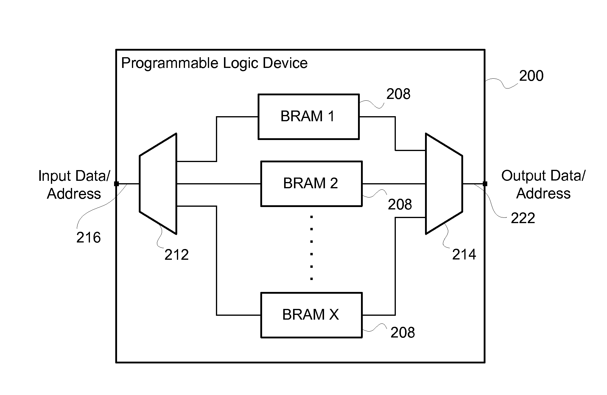
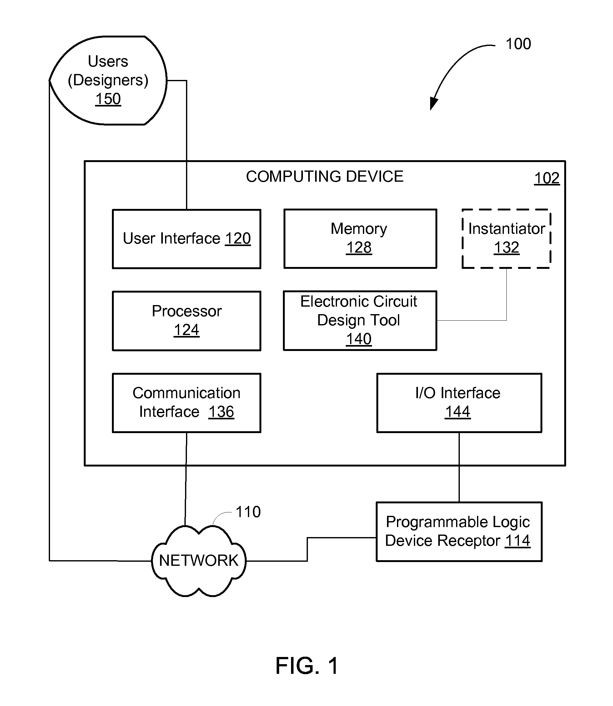
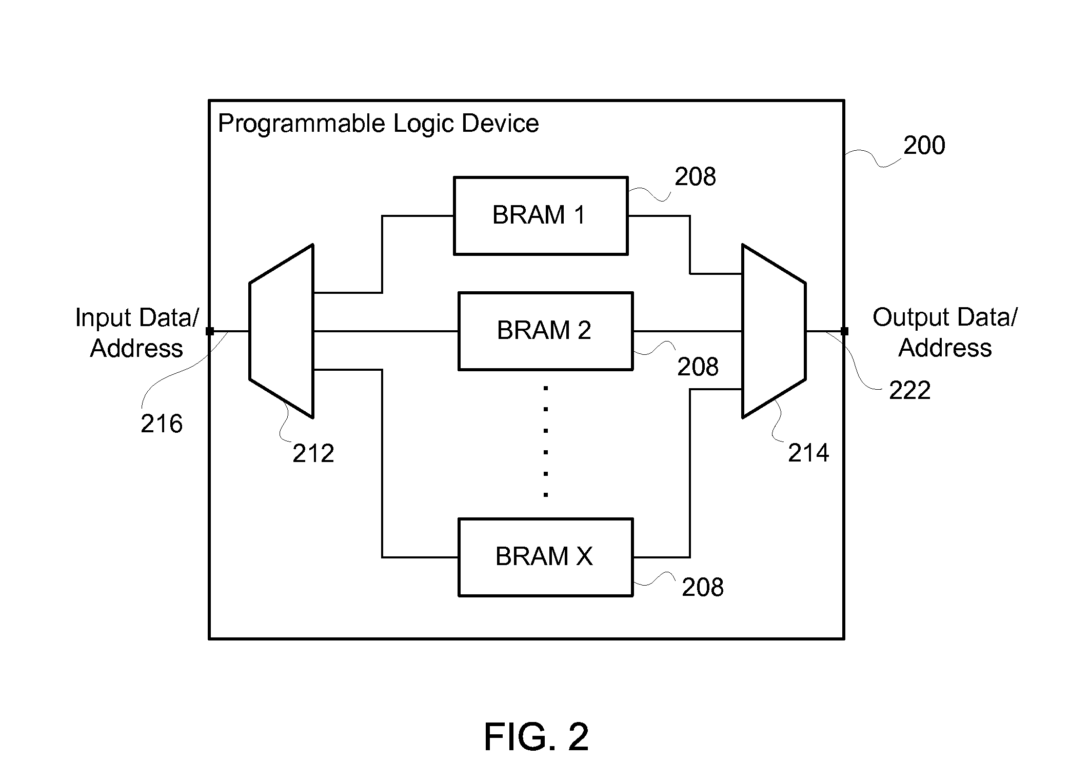
[0022]By way of introduction, the present disclosure relates to the instantiation of memory structures or blocks on programmable logic devices (PLDs). A memory management system, discussed in detail below, may automate the choice of which of a number of memory structures should be used, and if more than one is needed, to include the addressing and data multiplexing required to manage the instantiated memory in a way transparent to the end user of the PLD, regardless of the number of memory structures required. The end user may be a designer that may reconfigure the PLD without needing to understand the lower-level PLD design and without need to directly reconfigure the memory structures. The instantiation and memory management required by any given PLD design may be developed as part of the logic generated at the time of compilation of hardware description language (HDL) code in a system used to design, instantiate, and configure the logic blocks and interconnects of the PLD.

[0023]A...


PUM


Abstract

A system for memory instantiation in a programmable logic device (PLD) includes a computing device having a processor and memory coupled with the PLD. The processor is configured to receive memory parameters including at least a data width and a data depth. The processor is also configured to determine a number and sizes of block random access memory (BRAM) primitives required for data storage based on the memory parameters and based on one or more sizes of BRAM primitives available on the programmable logic device. In one example, the processor minimizes a size of the total number of BRAMs required for instantiation on the PLD. The processor is also configured to instantiate the determined number and corresponding sizes of the BRAM primitives in logic for configuration of the programmable logic device to include a device memory within the available BRAM primitives thereof corresponding to the determined number and sizes of the BRAM primitives.

Description

PRIORITY CLAIM[0001]This application claims the benefit of priority from U.S. Provisional Application No. 61 / 314,373, filed Mar. 16, 2010, which is incorporated herein by reference.BACKGROUND OF THE INVENTION[0002]1. Technical Field[0003]The present disclosure relates generally to programmable logic devices and, in particular, to a system for memory instantiation and management of block RAM on programmable logic devices.[0004]2. Related Art[0005]Programmable logic devices (PLDs) include field-programmable gate arrays (FPGAs), complex programmable logic devices (CPLDs), programmable array logic (PLAs), and generic array logic (GALs), among others, including reconfigurable systems. The PLDs are integrated circuits designed to be configured by a customer or designer after manufacturing. The PLD configuration is generally specified using a hardware description language (HDL), similar to that used for an application-specific integrated circuit (ASIC). PLDs may be used to implement any lo...

Claims


Application Information

Patent Timeline
IPC IPC(8): G06F12/02
CPCG06F17/5027G06F30/331
Inventor GELTER, AARONPARKER, BRIANBOATRIGHT, ROBERT
Owner HARMAN INT IND INC
Why Eureka
Try Eureka