
Low-Power Redundancy for Non-Volatile Memory

Active Publication Date: 2011-09-22
TEXAS INSTR INC
View PDF2 Cites 20 Cited by
  • Summary
  • Abstract
  • Description
  • Claims
  • Application Information

AI Technical Summary

Benefits of technology

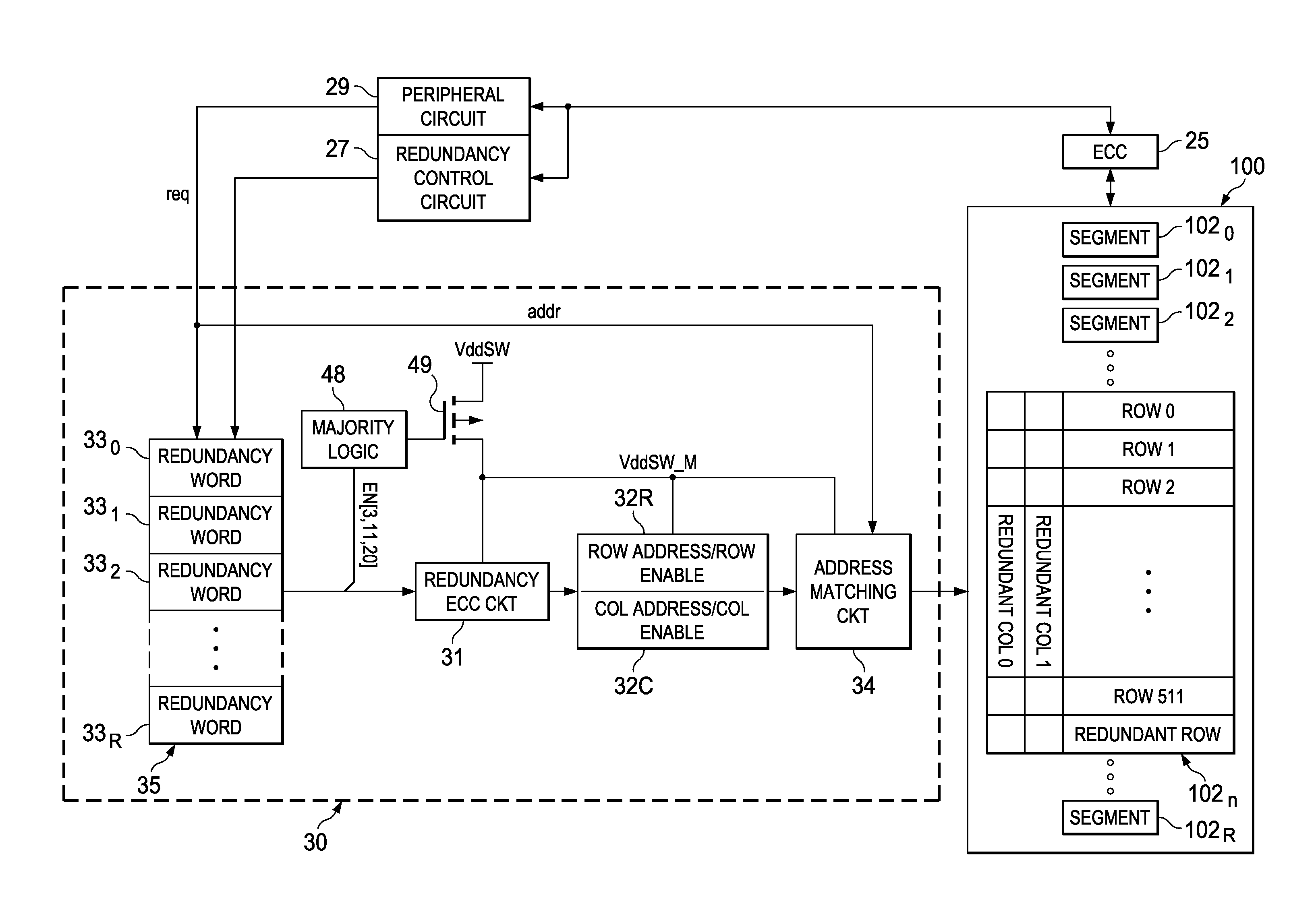
[0011]Embodiments of this invention provide a non-volatile memory with redundant memory elements, and a method of operating the same, in which the power requirements of the redundancy circuit selecting the main array or redundant memory cells are reduced.
[0014]Embodiments of this invention provide such a non-volatile memory and method that reduces vulnerability to soft-errors in the contents of the redundant memory.
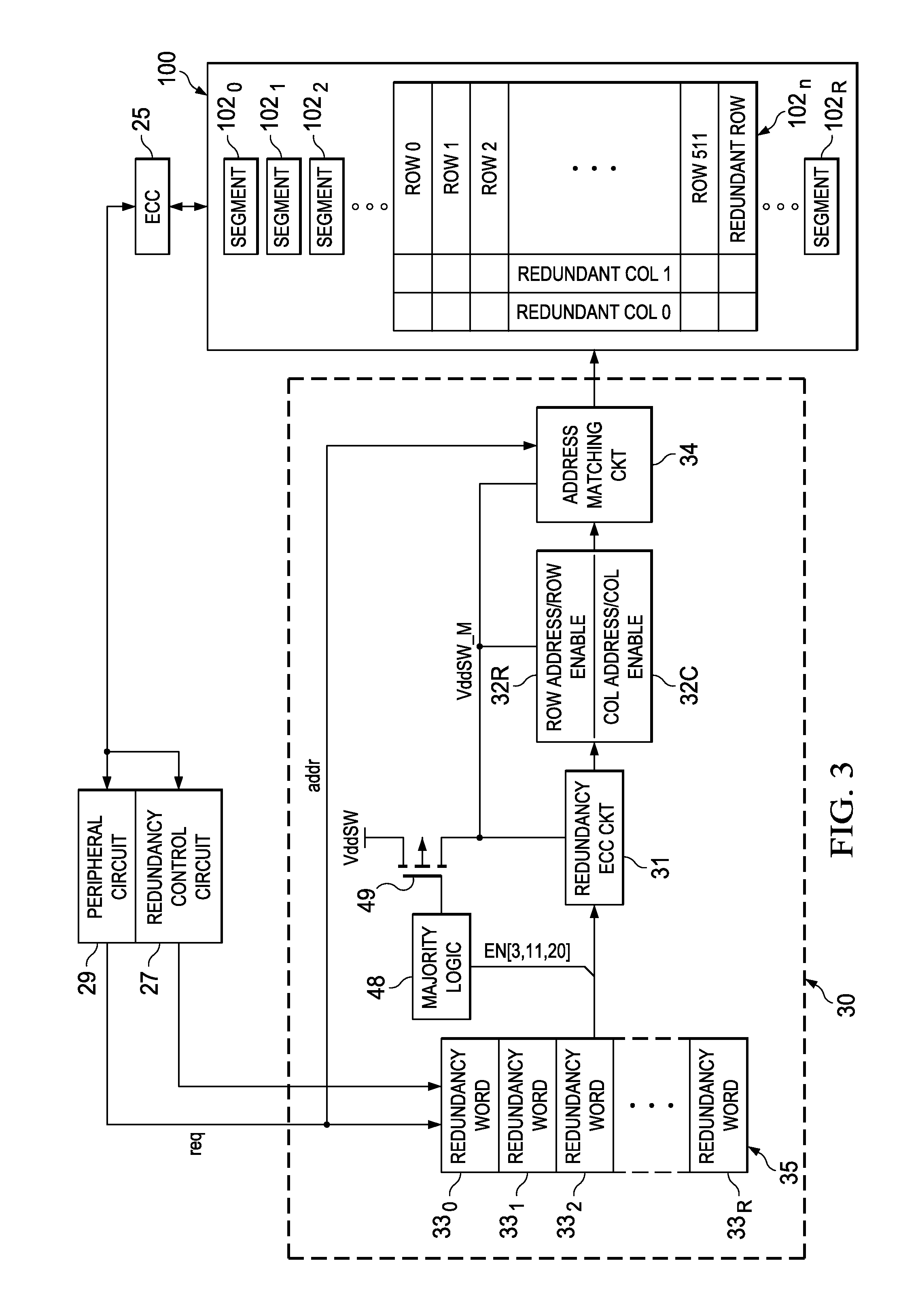
[0017]Embodiments of this invention may be realized by an integrated circuit containing a data array with redundant memory elements. A redundancy circuit that determines whether main memory array cells or redundant cells are accessed includes a static random access memory (SRAM) that stores the addresses to be replaced. Each data word in the redundancy SRAM includes the address to be replaced along with one or more enable bits indicating whether replacement is to be performed in the event of an address match. Power to the redundancy SRAM memory cells storing the addresses to be replaced is gated by the state of the enable bits. To the extent that redundancy is not enabled, power consumption in the redundancy SRAM is reduced.
[0018]According to another aspect of the invention, multiple redundant elements (rows and columns) are available for each main memory array segment, each associated with an address and an enable bit. The enabling of any one of the multiple redundant elements enables all redundant elements for the segment. An enable signal for the segment is generated from a “majority encoding” of the multiple enable bits. Vulnerability to soft-error failure of a single redundant enable bit in the redundancy SRAM is thus eliminated.

Problems solved by technology

The power consumption of the electronic circuitry in those devices and systems is therefore of great concern, as battery life is often a significant factor in the buying decision as well as in the utility of the device or system.
Given the substantial memory capacity now required by these computationally sophisticated, a significant portion of the overall chip area is consumed in realizing solid-state memory, particularly non-volatile solid-state memory, even in large-scale SoC implementations.
The manufacturing yield of modern SoC integrated circuits is thus often dominated by manufacturing defects in the memory arrays, considering that a relatively large portion of the overall chip area is consumed by the memory arrays, and that the memory arrays are constructed of a large number of closely-packed, minimum feature size, memory cells.
A defective embedded on-chip memory causes the entire SoC to be unsuitable for system use, regardless of the functionality of the remainder of the integrated circuit.
It has been observed, however, that significant power remains being consumed by the SRAM redundancy memory, considering that this memory has at least one data word for each segment of the non-volatile array.

Method used


Image

  • Low-Power Redundancy for Non-Volatile Memory
  • Low-Power Redundancy for Non-Volatile Memory
  • Low-Power Redundancy for Non-Volatile Memory

Examples


Embodiment Construction

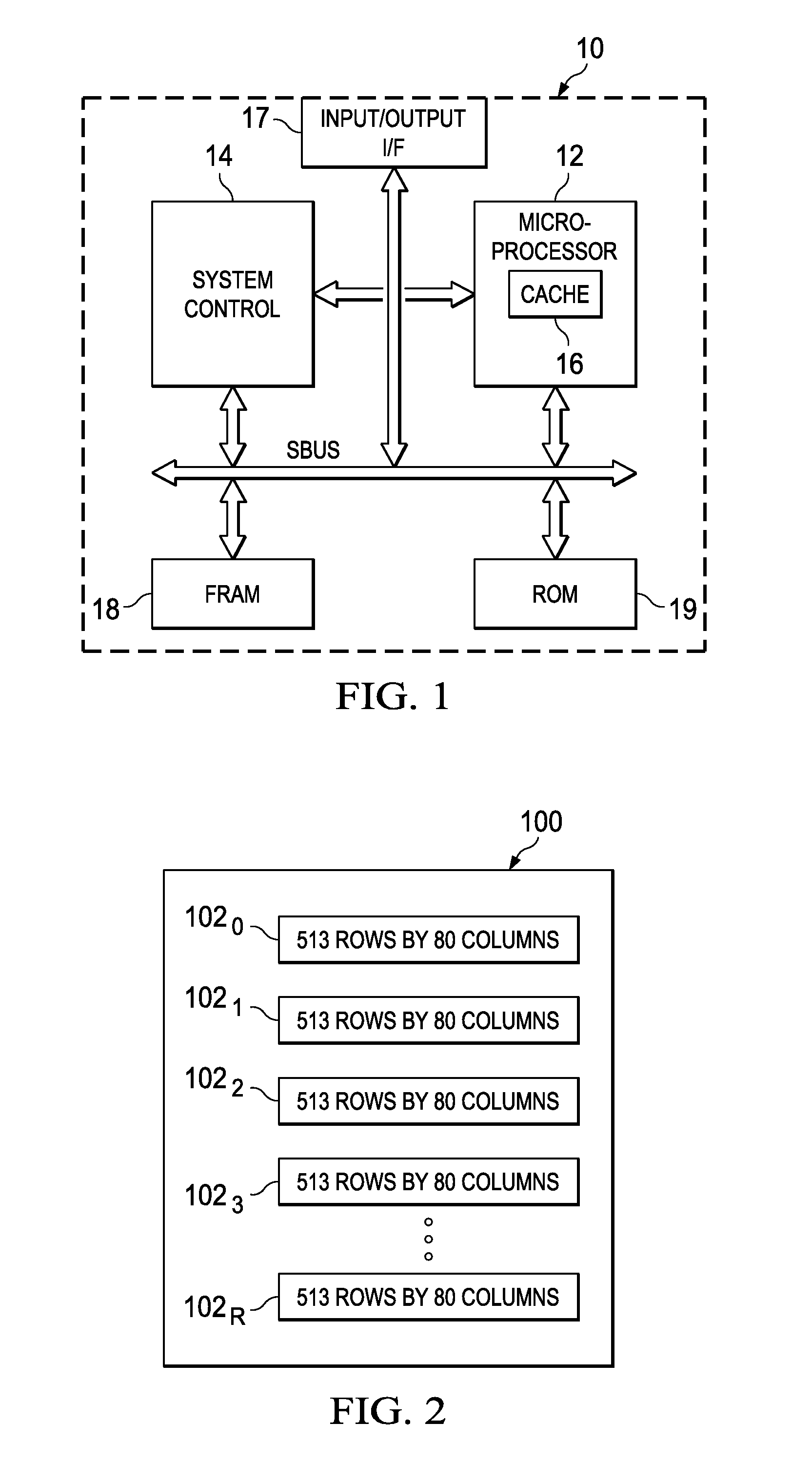
[0026]The present invention will be described in connection with its embodiments, namely as implemented into an integrated circuit including a ferroelectric random access memory (FRAM, or FeRAM), because it is contemplated that this invention will be of particular benefit in such an application. However, it is also contemplated that this invention may be used to advantage in other memory and integrated circuit architectures beyond that described herein. Accordingly, it is to be understood that the following description is provided by way of example only, and is not intended to limit the true scope of this invention as claimed.

[0027]Modern solid-state memory is realized by various memory technologies. Static random access memory (SRAM) is now commonplace in many modern electronic systems. As is fundamental in the art, SRAM cells store data “statically”, in that the stored data state remains latched in each cell so long as power is applied to the memory. Typically, each SRAM cell is c...


PUM


Abstract

A static RAM redundancy memory for use in combination with a non-volatile memory array, such as ferroelectric RAM (FRAM), in which the power consumption of the SRAM redundancy memory is reduced. Each word of the redundancy memory includes data bit cells for storing addresses of memory cells in the FRAM array to be replaced by redundant elements, and also enable bits indicating whether redundancy is enabled for those addresses. A logical combination of the enable bits in a given word determines whether the data bit cells in that word are powered-up. As a result, the power consumption of the redundancy memory is reduced to the extent that redundancy is not enabled for segments of the FRAM array.

Description

CROSS-REFERENCE TO RELATED APPLICATIONS[0001]This application claims priority, under 35 U.S.C. §119(e), of Provisional Application No. 61 / 315,201, filed Mar. 18, 2010, incorporated herein by this reference.STATEMENT REGARDING FEDERALLY SPONSORED RESEARCH OR DEVELOPMENT[0002]Not applicable.BACKGROUND OF THE INVENTION[0003]This invention is in the field of solid-state memory as realized in semiconductor integrated circuits. Embodiments of this invention are more specifically directed to the use of redundant memory cells to functionally replace defective memory cells in such memories.[0004]Many modern electronic devices and systems now include substantial computational capability for controlling and managing a wide range of functions and useful applications. Many of these electronic devices and systems are now portable or handheld devices. For example, many mobile devices with significant computational capability are now available in the market, including modern mobile telephone handse...

Claims


Application Information

Patent Timeline
IPC IPC(8): G11C7/22H03M13/05G06F11/10
CPCG06F11/1016G11C7/02G11C29/84G11C29/789G11C29/83G11C11/22
Inventor TOOPS, DAVID J.MADAN, SUDHIR K.BALASUBRAMANIAN, SURESH
Owner TEXAS INSTR INC
Learn More