Integrated touch panel and manufacturing method thereof

a touch panel and integrated technology, applied in the field of touch panel technology, can solve the problems of high price affecting the quality of the image on the display, and incomplete or uneven cladding, so as to improve the strength and stability of the touch panel, reduce the resolution, and increase the yield of the structure

Inactive Publication Date: 2011-09-29
APPLIED VACUUM COATING TECH +1
View PDF13 Cites 27 Cited by
  • Summary
  • Abstract
  • Description
  • Claims
  • Application Information

AI Technical Summary

Benefits of technology

[0008]In view of the abovementioned problems, the purpose of the present invention is to coat on one of an icon or artwork layer on the periphery of one side face of the transparent substrate, also the inner periphery of the icon or artwork layer is not perpendicular to the adjacent line of the transparent substrate. Sputtering method is then used to stack layers of optical films or sensing layers on the above. As the icon layer or artwork layer is not placed perpendicularly, complete cladding of the optical films or sensing layers can be done and thus the yield rate of the device increased.
[0016]The other purpose of the present invention is to propose a production method for the abovementioned integrated touch panel. The temperature of the entire production process has to be controlled below 200° C. in order to greatly enhance the strength and stability of the touch panel. The production steps include cutting the transparent substrate into a few pieces and coating an icon layer on the periphery of each transparent substrate. The inner periphery of each icon layer or artwork layer is not perpendicular to the adjacent line of such transparent substrate. A sensing layer is coated on each icon layer or artwork layer and the areas on the transparent substrate which are not coated with icon layer or artwork layer via sputtering method. However, prior to and / or after the stacking of the sensing layer, at least one layer of optical film may be formed and placed on one side face or two side face of the sensing layer.
[0017]One of the advantages of the present invention is that instead of using the conventional way of laminating the transparent substrate and sensing layer with optically clear adhesive, the inner periphery of the icon layer or artwork layer is arranged not perpendicular to the adjacent line of the transparent substrate so that a complete cladding of the optical film or sensing layer can be done via sputtering method. The yield of the structure is thus raised. At the same time, one layer or two layers of optical film are covered on the top and / or bottom surface of each sensing layer. This addition will cover up the metal slots caused by circuit etching preventing them from reducing the resolution and impairing the visual quality of the touch panel.

Problems solved by technology

Therefore, the panels come at a high price.
The conventional icon layer is printed on the cover glass substrate perpendicularly and this will usually cause unsatisfactory results when laminating the substrate to the sensing layer; incomplete or uneven cladding may occur.
Many times, the uneven slots produced during the etching of sensing circuits on the ITO sensing layers will compromise the quality of the images on the display and reduce its yield rate.

Method used


Image

  • Integrated touch panel and manufacturing method thereof
  • Integrated touch panel and manufacturing method thereof
  • Integrated touch panel and manufacturing method thereof

Examples


first embodiment

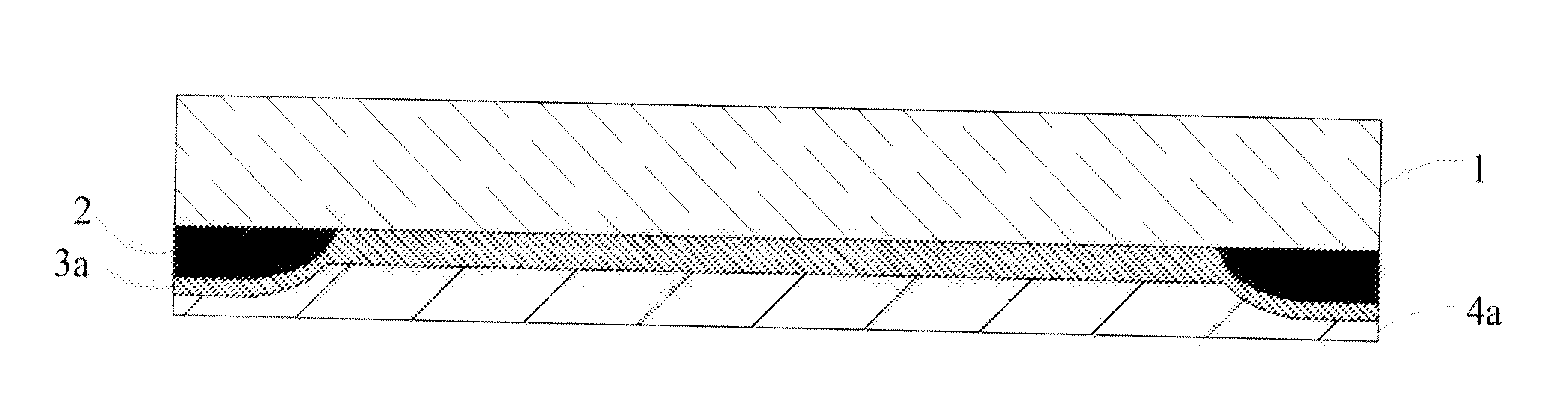
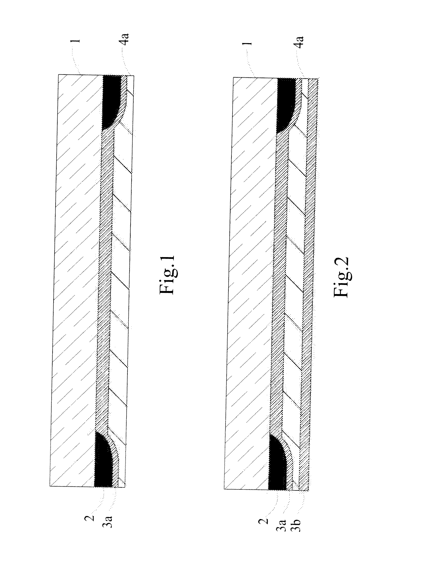
[0041]Please refer to the first drawing (FIG. 1). FIG. 1 shows the cross section view of the present invention. As shown in the drawing, the embodiment is the structure of an integrated touch panel. Combining a display panel (not shown in the drawing) with it will create a complete panel. This integrated touch panel is made up of a transparent substrate 1, an icon layer or an artwork layer 2, a first layer of optical film 3a, and a first sensing layer 4a.

[0042]The transparent substrate 1 is the outermost surface of the touch panel that directly comes to contact with the environment. Therefore, it is strengthened to protect it from scratch and other damages. The transparent substrate 1 may either be made from glass or polymer plastic. If glass is used as its material, the glass is first cut into several small pieces where the thickness of each is about 0.5˜1.8 mm. These little pieces are then chemically-tempered by dipping them in potassium nitrate solution or other chemical solutio...

third embodiment

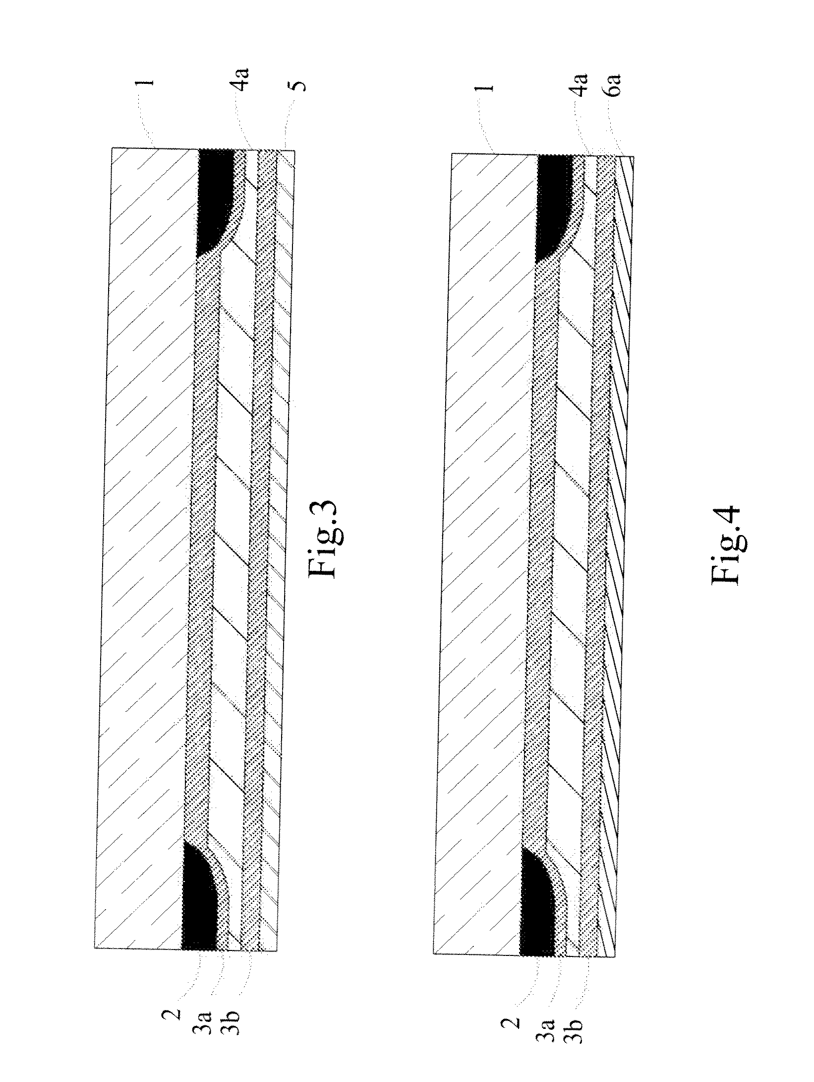
[0063]Please refer to the nineteenth drawing (FIG. 19). FIG. 19 shows the cross section view of the present invention. As shown in the drawing, the embodiment is the structure of an integrated touch panel combined with a display panel (not shown in the drawing) forming a complete panel. The integrated touch panel is made up of one transparent substrate 1 and one icon layer 2 coated on the periphery of one side face of the transparent substrate 1. The inner edge of the icon layer or artwork layer 2 is not perpendicular to the adjacent line of the transparent substrate 1. It also consists of the first layer of optical film 3a which is stacked on the abovementioned icon layer or artwork layer 2 and the areas on the transparent substrate 1 which are not coated with icon layer or artwork layer 2. Other than that, it consists of the first sensing layer 4a which is stacked on the above optical film 3a via sputtering method. A second layer of optical film 3b is stacked on the first sensing ...


PUM

PropertyMeasurementUnit
temperatureaaaaaaaaaa
thickaaaaaaaaaa
viscosityaaaaaaaaaa

Abstract

The present invention provides an integrated touch panel comprising a transparent substrate, one of an icon or artwork layer, a first layer of optical film, and a first sensing layer. The icon layer or artwork layer is coated on the periphery of one side face of the transparent substrate, and the inner periphery of the icon layer or artwork layer is not perpendicular to the adjacent line of the transparent substrate. The first layer of optical film is stacked on icon layer or artwork layer and the areas on the transparent substrate uncovered with icon layer. The first sensing layer is stacked on the first layer of optical film by sputtering. The interchangeability is included in the patent claim of the present invention. As icon layer or artwork layer is not perpendicular to the transparent substrate, the subsequent cladding of the structures may be completed by sputtering or other methods.

Description

CROSS-REFERENCE TO RELATED APPLICATIONS[0001]This non-provisional application claims priority under 35 U.S.C. §119(a) on Patent Application No(s). 099109075 filed in Taiwan, R.O.C. on Mar. 26, 2010, the entire contents of which are hereby incorporated by reference.BACKGROUND OF THE INVENTION[0002]1. Field of the Invention[0003]The present invention is related to the touch panel technology, specifically in the invention of an integrated touch panel of which production process is simplified, panel strength is intensified, and yield rate is increased.[0004]2. Description of the Related Art[0005]There are some common types of touch panels; i.e. the resistive panel, capacitive panel, surface acoustic wave panel, optical (infrared) panel etc. Among these, the most commonly used are the resistive panels, followed by the capacitive panels. The advantages of the capacitive panels are waterproofing and scratch-proofing, and they have high light transmittance and broad temperature range. There...

Claims


Application Information

Patent Timeline
Patent Type & Authority Applications(United States)
IPC IPC(8): G06F3/041C23C14/34
CPCG06F2203/04103G06F3/044G06F3/0445
Inventor CHOU, SHIH-LIANGCHIANG, HSUEH-CHIHWENG, CHIEN-MINCHU, TZU-WENWANG, FU-JENLEE, I-WENCHEN, HSING-YEH
Owner APPLIED VACUUM COATING TECH
Why Eureka
Try Eureka