

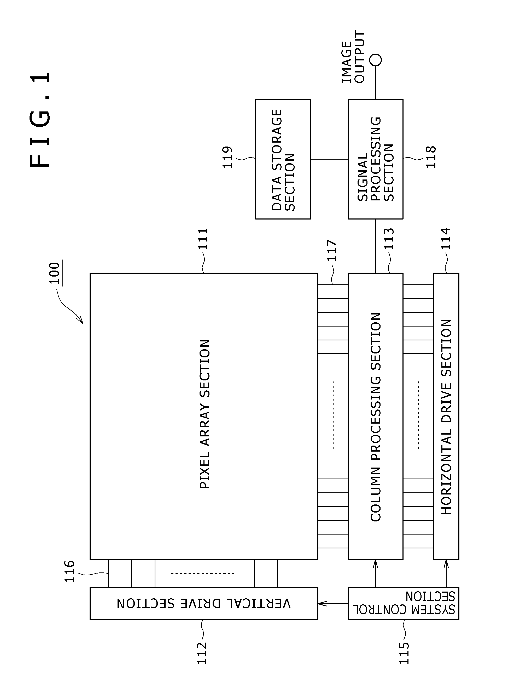
Solid-state imaging device, method of manufacturing solid-state imaging device, and electronic apparatus
a solid-state imaging and imaging device technology, applied in the direction of radio frequency controlled devices, transistors, television systems, etc., can solve the problems of deterioration of image quality, image distorted, and decrease of the maximum amount of electric charge (maximum charge amount) that can be accumulated in the photodiode, so as to achieve high image quality and high quality
- Summary
- Abstract
- Description
- Claims
- Application Information
AI Technical Summary
Benefits of technology
Problems solved by technology
Method used
Image

Examples
first embodiment
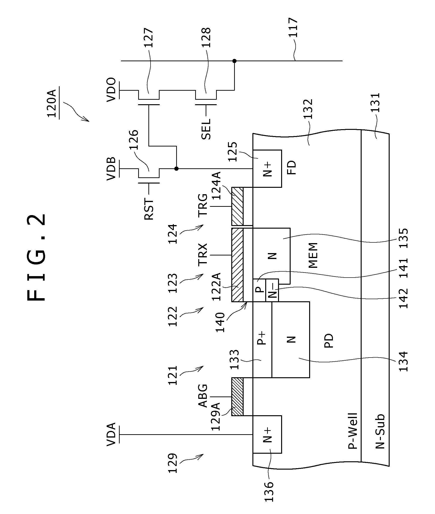
[0099]Now, the configuration of unit pixels 120A in a first embodiment will be described below referring to FIGS. 3 to 5. In FIGS. 3 to 5 and in the following drawings, the same components as those in the unit pixel of FIG. 2 will be denoted by the same reference symbols as used in FIG. 2, and detailed descriptions of them will be omitted.
[0100]FIG. 3 is a plan view showing the configuration of a unit pixel 120A.
[0101]As shown in FIG. 3, a photodiode 121, a memory part 123, and a floating diffusion region 125 are disposed in the unit pixel 120A. The photodiode 121 and the memory part 123 are formed to have such an impurity concentration that a depletion state is obtained upon discharging of electric charge. The floating diffusion region 125 is formed to have an impurity concentration such as to permit electrical connection therewith of a wiring contact for taking out a voltage.
[0102]Besides, in the unit pixel 120A, a first transfer gate 122 is provided between the photodiode 121 and...
second embodiment
[0155]Now, a unit pixel 120B according to a second embodiment will be described below, referring to FIGS. 12A to 13B. FIG. 12A is a plan view showing the configuration of the unit pixel 120B, and FIG. 12B is a sectional view of the unit pixel 120B along line Z-Z′ of FIG. 12A. Besides, FIG. 13A shows the potential state along line X-X′ of FIG. 12A which passes through a complete transfer path 150, and FIG. 13B shows the potential state along line Y-Y′ of FIG. 12 which passes through an intermediate transfer path 140.
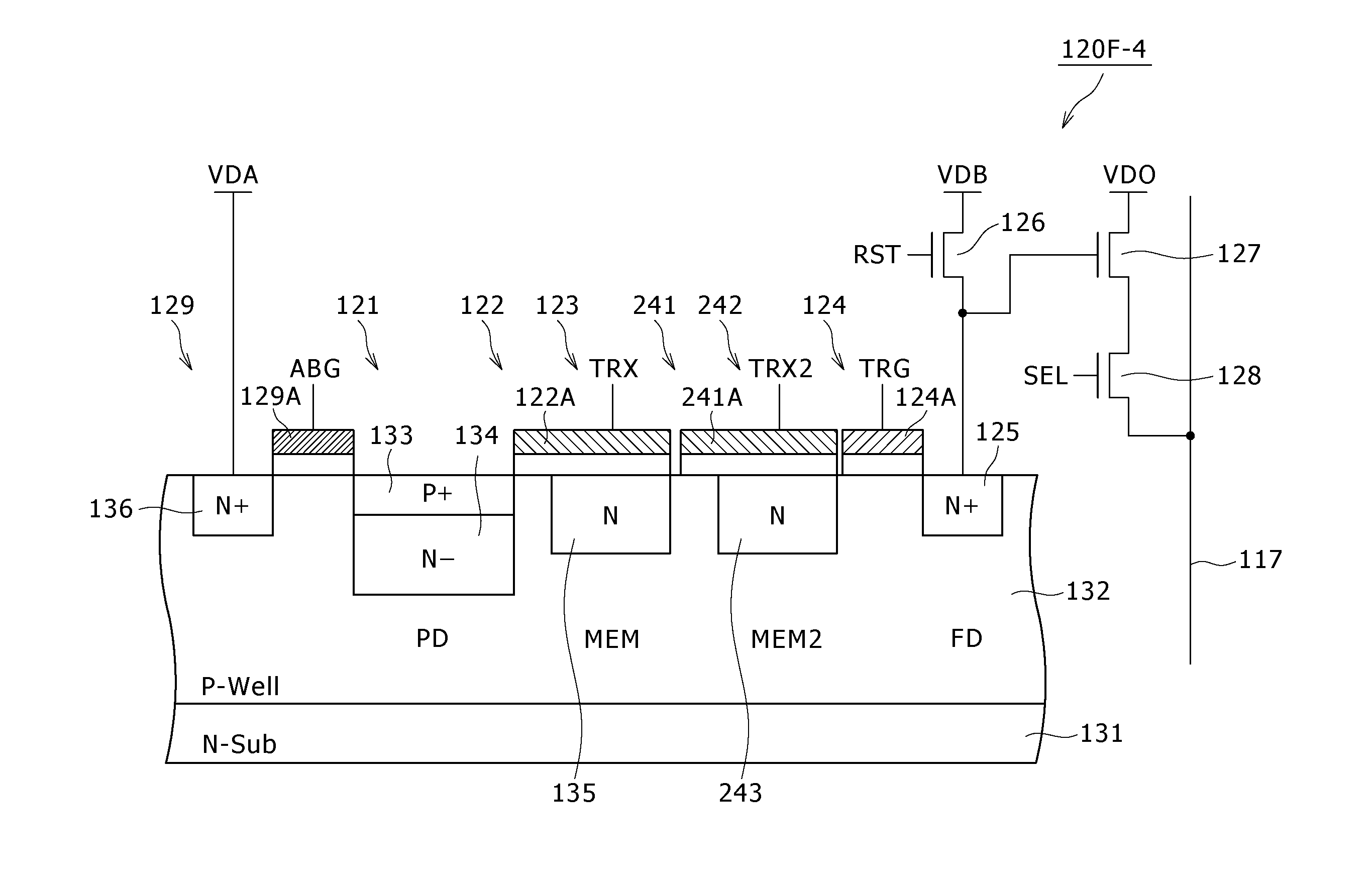
[0156]In the unit pixel 120B, an N-type buried layer 134 of a photodiode 121 and a buried channel 135 of a memory part 123 are formed so that a part of the N-type buried layer 134 and a part of the buried channel 135 overlap, in plan view, with each other over the whole surface in the width direction (the vertical direction in FIG. 12A) at a boundary portion between the photodiode 121 and the memory part 123. Besides, in a separation region between them in the depth direc...
third embodiment
[0161]Now, a unit pixel 120C according to a third embodiment will be described below, referring to FIGS. 15A and 15B. FIG. 15A is a plan view showing the configuration of the unit pixel 120C, and FIG. 15B is a sectional view of the unit pixel 120C along line Z-Z′ of FIG. 12A.
[0162]In the unit pixel 120C, an N-type buried layer 134 of a photodiode 121 is so formed as to extend to the lower side (the deep side in the substrate) of a part or the whole part of the memory part 123. Thus, the N-type buried layer 134 is formed to be L-shaped in the section shown in FIG. 15B. Besides, in the unit pixel 120C, an impurity diffusion region 142 is formed at a boundary portion between the lower surface of a buried channel 135 of the memory part 123 and the upper surface of the N-type buried layer 134 extending to the lower side of the memory part 123, whereby an intermediate transfer path 140 is provided.
[0163]With the impurity diffusion region 142 thus formed at the boundary portion between the...
PUM
| Property | Measurement | Unit |
|---|---|---|
| electric charge | aaaaa | aaaaa |
| concentration | aaaaa | aaaaa |
| conductivity | aaaaa | aaaaa |
Abstract
Description
Claims
Application Information