Forming a compound-nitride structure that includes a nucleation layer

a compound-nitride and nucleation layer technology, applied in the direction of coatings, semiconductor devices, chemical vapor deposition coatings, etc., can solve the problems of affecting the performance of the device, affecting the practicality of the device fabrication, and affecting the device performan

Inactive Publication Date: 2011-10-06
APPLIED MATERIALS INC
View PDF2 Cites 50 Cited by
  • Summary
  • Abstract
  • Description
  • Claims
  • Application Information

AI Technical Summary

Benefits of technology

[0009]In one embodiment, a method for fabricating a compound nitride-based semiconductor structure is provided. The method comprises forming a Group III-nitride buffer layer, or nucleation layer, over one or more substrates in a first processing chamber, transferring the one or more substrates having the Group III-nitride buffer layer deposited thereon into a second processing chamber without exposing the one or more substrates to an ambient atmospheric environment, and forming a bulk Group III-V layers over the Group III-nitride buffer layer in the second processing chamber. In one example, the first processing chamber may be a MOCVD, PVD, CVD, ALD, sputtering chamber, or any other vapor deposition chamber. The second processing chamber may be a MOCVD or HVPE chamber.
[0010]In another embodiment, a method for fabricating a compound nitride-based semiconductor structure is provided. The method comprises forming a Group III-nitride buffer layer over one or more silicon-based substrates in a first processing chamber containing a Ga-free environment, transferring the one or more silicon-based substrates having the Group III-nitride buffer layer deposited thereon, without exposing the one or more substrates to an ambient atmospheric environment, into a second processing chamber containing an Al-free environment, and forming a bulk Group III-V layer over the Group III-nitride buffer layer in the second processing chamber. In one example, the first processing chamber may be a MOCVD, PVD, CVD, ALD, sputtering chamber, or any other vapor deposition chamber. The second processing chamber may be a MOCVD or HVPE chamber.
[0011]In one another embodiment, a processing system for processing compound nitride-based semiconductor devices is provided. The processin

Problems solved by technology

While the feasibility of using GaN to create photoluminescence in the blue region of the spectrum has been known for decades, there were numerous barriers that impeded their practical fabrication.
For example, lattice mismatch issues often occur between the sapphire substrate and the Group III-nitride layer due to their significant differences in the lattice constant, thermal expansion coefficient, and interfacial surface energy.
Dislocations may propagate from these lattice mismatch sites through t

Method used


Image

  • Forming a compound-nitride structure that includes a nucleation layer
  • Forming a compound-nitride structure that includes a nucleation layer
  • Forming a compound-nitride structure that includes a nucleation layer

Examples


Embodiment Construction

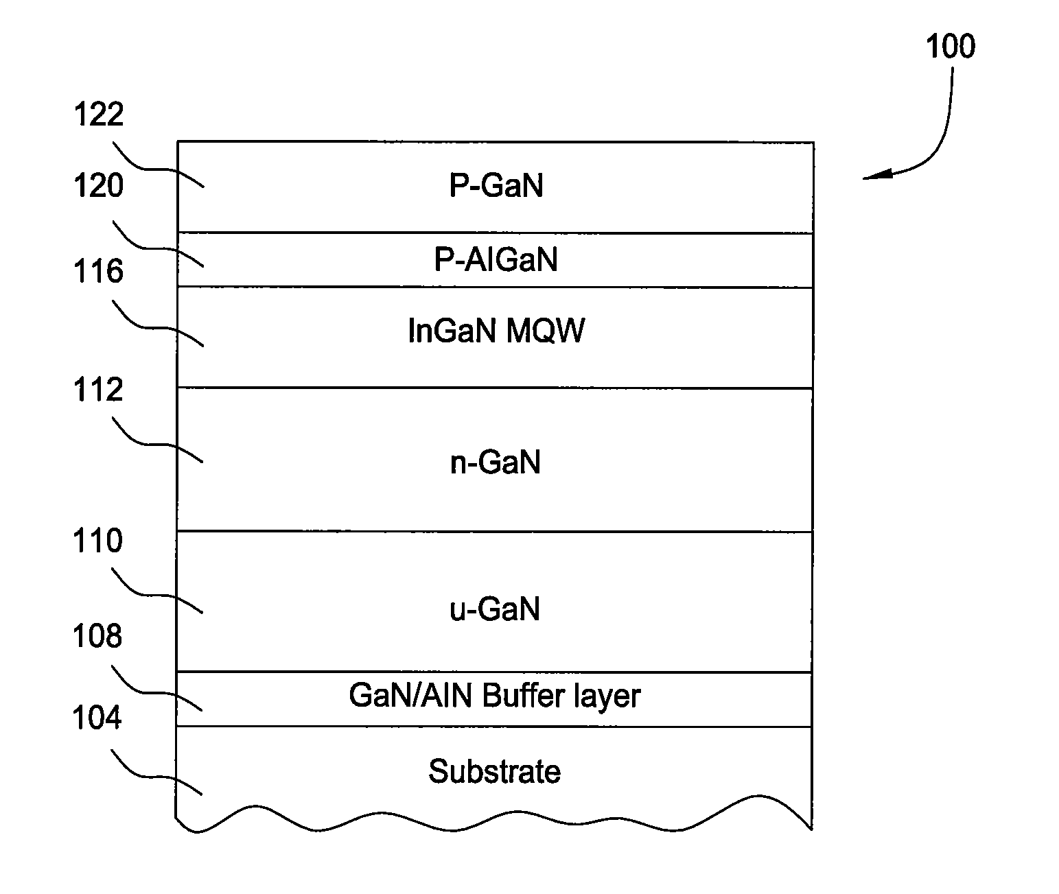
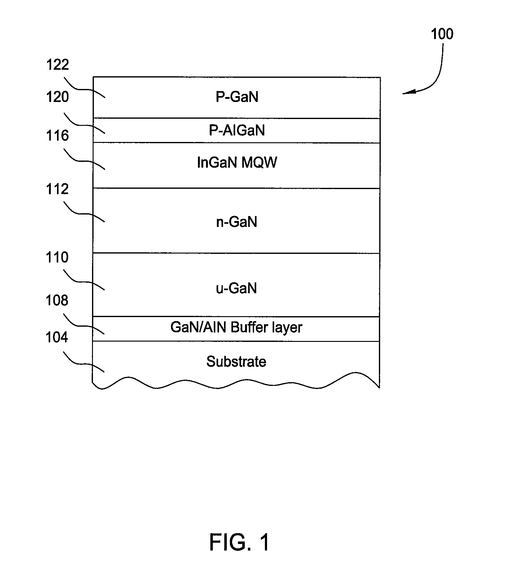
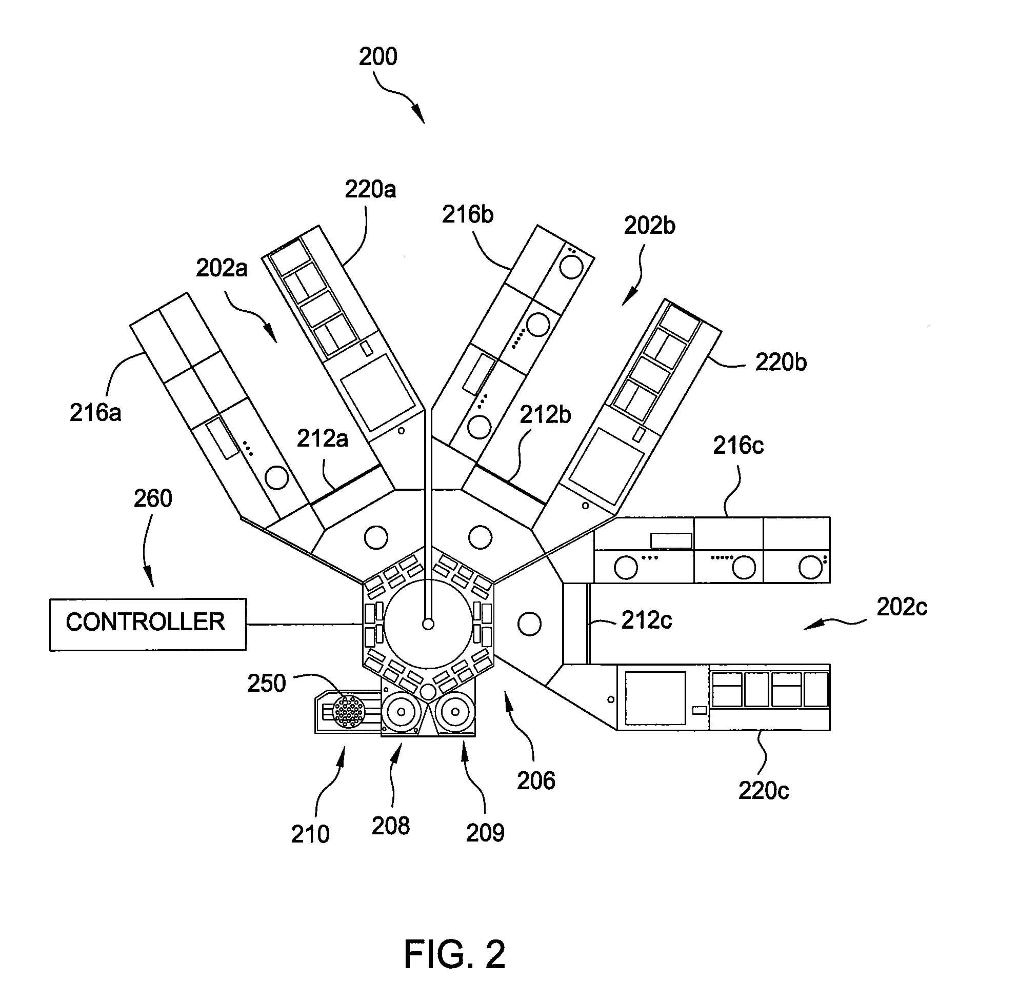
[0021]Embodiments described herein generally relate to methods for forming Group III-V materials by metal organic chemical vapor deposition (MOCVD) or hydride vapor phase epitaxial (HVPE) processes. In one embodiment, a separate processing chamber is adapted to grow buffer layers, or sometimes referred to as nucleation layers, for the subsequent growth of Group III-V layers at a higher temperature in another processing chamber. In another embodiment, a separate processing chamber is adapted to grow Ga-free AlN buffer layer on a silicon-based substrate for the subsequent growth of Group III-V layers in another processing chamber containing an Al-free environment. A dedicated processing chamber is beneficial to film properties of the buffer layer since growth characteristics such as density of nucleation islands, island size, thickness, etc. are exactly controlled. Meanwhile, the system throughput may be increased by eliminating cleaning and adjustment to the process chambers as would...


PUM

PropertyMeasurementUnit
Temperatureaaaaaaaaaa
Semiconductor propertiesaaaaaaaaaa

Abstract

The present invention generally provides apparatus and methods for forming LED structures. In one embodiment, a method for fabricating a compound nitride-based semiconductor structure is provided. The method comprises forming a Group III-nitride buffer layer over one or more substrates in a first processing chamber, transferring the one or more substrates having the Group III-nitride buffer layer deposited thereon into a second processing chamber without exposing the one or more substrates to an ambient atmospheric environment, and forming a bulk Group III-V layers over the Group III-nitride buffer layer in the second processing chamber. In one example, the first processing chamber may be a MOCVD, PVD based chamber, CVD based chamber, ALD based chamber, sputtering chamber, or any other vapor deposition chamber. The second processing chamber may be a MOCVD or HVPE chamber.

Description

CROSS-REFERENCE TO RELATED APPLICATIONS[0001]This application claims benefit of U.S. provisional patent application Ser. No. 61 / 320,234 [Attorney Docket No.: APPM 14823L], filed Apr. 1, 2010, which is herein incorporated by reference.BACKGROUND OF THE INVENTION[0002]1. Field of the Invention[0003]Embodiments of the present invention generally relate to the manufacturing of devices, such as light emitting diodes (LEDs), laser diodes (LDs) and, more particularly, to processes for forming Group III-V materials by metal-organic chemical vapor deposition (MOCVD) or hydride vapor phase epitaxial (HVPE) processes.[0004]2. Description of the Related Art[0005]Group III-V films are finding greater importance in the development and fabrication of a variety of semiconductor devices, such as short wavelength LEDs, LDs, and electronic devices including high power, high frequency, high temperature transistors and integrated circuits. For example, short wavelength (e.g., blue / green to ultraviolet) ...

Claims


Application Information

Patent Timeline
IPC IPC(8): H01L21/20
CPCC23C16/301C23C16/303C23C16/54H01L21/0237H01L33/007H01L21/02505H01L21/0254H01L21/0262H01L21/02458H01L33/00
Inventor SU, JIE
Owner APPLIED MATERIALS INC
Why Eureka
Try Eureka