Microelectrode array architecture

a technology of array architecture and microelectrode, which is applied in the field of microelectrode array architecture, can solve the problems of high cost of semiconductor manufacturing techniques, difficult access to semiconductor foundries, so as to reduce labor and cost, reduce energy consumption, and relieve loc designers

Inactive Publication Date: 2011-10-13
SPARKLE POWER
View PDF1 Cites 77 Cited by
  • Summary
  • Abstract
  • Description
  • Claims
  • Application Information

AI Technical Summary

Benefits of technology

[0028]In another embodiment, the interconnection of the microelectrodes and the system control circuitry is arranged in a daisy chain configuration to minimize the number of necessary interconnections. The number of interconnections will be the bottle neck of scaling down the size of the microelectrode and scaling up the total number of the microelectrodes.
[0029]Still in another embodiment, a passive top cover plate, an active top cover plate which works as ground, or another coplanar microelectrode array as the top cover plate can be employed in the microelectrode array architecture. A passive cover plate means no electrical circuitry on the plate and it could be just a transparent cover to seal the test surface for the protection of the fluidic operations or for the purpose of protecting the test medium for a longer shelf storage life. Even though a conventional bi-planar structure, which includes two active parallel plates, is less desirable but still can be employed in the Microelectrode Array Architecture. In this case, the top plate is coated with a continuous ground electrode which has the combined features of electrical conductivity and optical transparency in a thin layer. Still the more advanced top cover plate can be implemented by another coplanar microelectrode array which is turned upside down. In all the cases, when the manipulation of droplets in which the top cover plate is implemented in the Microelectrode Array Architecture, the distance between the top and lower plates, called the gap, is adjustable. This capability of the Microelectrode Array Architecture is especially powerful and provides more flexibility to the manipulations of the droplets under the coplanar structure.
[0031]In one embodiment, the Microelectrode Array Architecture can be used to implement a Field-programmable LOC (FPLOC). The field programmability of FPLOC can significantly reduce the labor and cost associated with generating the digital microfluidic systems by relieving LOC designers from the burden of manual optimization of bioassays, time-consuming hardware design, costly testing and maintenance procedures. FPLOC is analogue to FPGA in ASIC design. A turn of modifications of custom-hardwired LOC (like ASIC) takes several months, but a turn of modifications of a design for FPLOC (like FPGA) only takes minutes to hours.
[0032]In one embodiment, a Field-programmable Permanent Display is implemented by the Microelectrode Array Architecture. A Field-programmable Permanent Display is a display which can be programmed by software but after the programming the power to the display can be turned off and the display will stay on permanently. The lowness of energy consumption and no sustaining power required for the Field-programmable Permanent Display is a big advantage over other display technologies. Many applications can utilize the Field-programmable Permanent Display invention. The test results of a FPLOC, which is based on the same Microelectrode Array Architecture, can be shown easily using Field-programmable Permanent Display as records. Field-programmable newspapers or books, or posters, billboards, pictures, signs etc. are among the obvious applications.

Problems solved by technology

These techniques offer many advantages in the implementation of the digital microfluidics paradigm as described above but current fabrication techniques to produce these microfluidic chips still depend on rather complex and expensive manufacturing techniques.
In addition to higher cost for semiconductor manufacturing techniques, semiconductor foundries are not easily accessible.
Unfortunately, the conventional microfluidic systems employing microfluidic technique built to date are still highly specialized to particular applications.
The progress in microfluidic system development (including both continuous-flow and digital microfluidic devices) has been hampered by the absence of standard commercial components.
Also, due to the fixed layouts of current microfluidic chips, a new chip design is required for each application, making it expensive to develop new applications.
Furthermore, many of these devices are fabricated using expensive microfabrication techniques derived from semiconductor integrated circuit manufacturing.
As a result, applications for microfluidic devices are expanding relatively slowly due to the cost and effort required to develop new devices for each specific application.
Although batch fabrication allows microfabricated devices to be inexpensive when mass-produced, the development of new devices can be prohibitively expensive and time consuming due to high prototyping costs and long turn-around time associated with fabrication techniques.
Also, as more bioassays are executed concurrently on a LOC as well as more sophisticated control for resource management, system integration and design complexity are expected to increase dramatically.
The difficulty with a hierarchical approach is the lack of standard fabrication technologies and digital microfluidic device simulation libraries, which make the hierarchical design approach difficult to implement.

Method used


Image

  • Microelectrode array architecture
  • Microelectrode array architecture
  • Microelectrode array architecture

Examples


Embodiment Construction

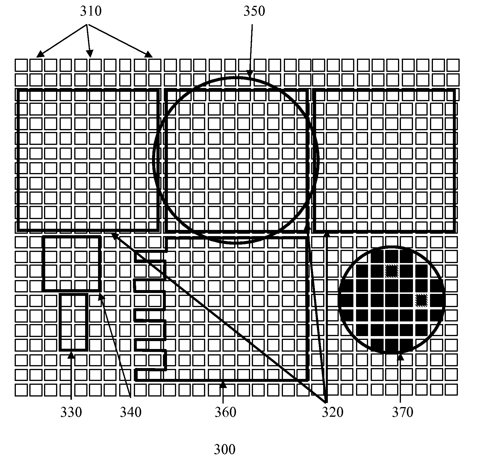
[0096]Microelectrode Array Architecture can be applied to other digital microfluidic technologies such as dielectrophoresis (DEP) based technologies but for the discussions below, EWOD technology will be used to illustrate various embodiments of the present invention.

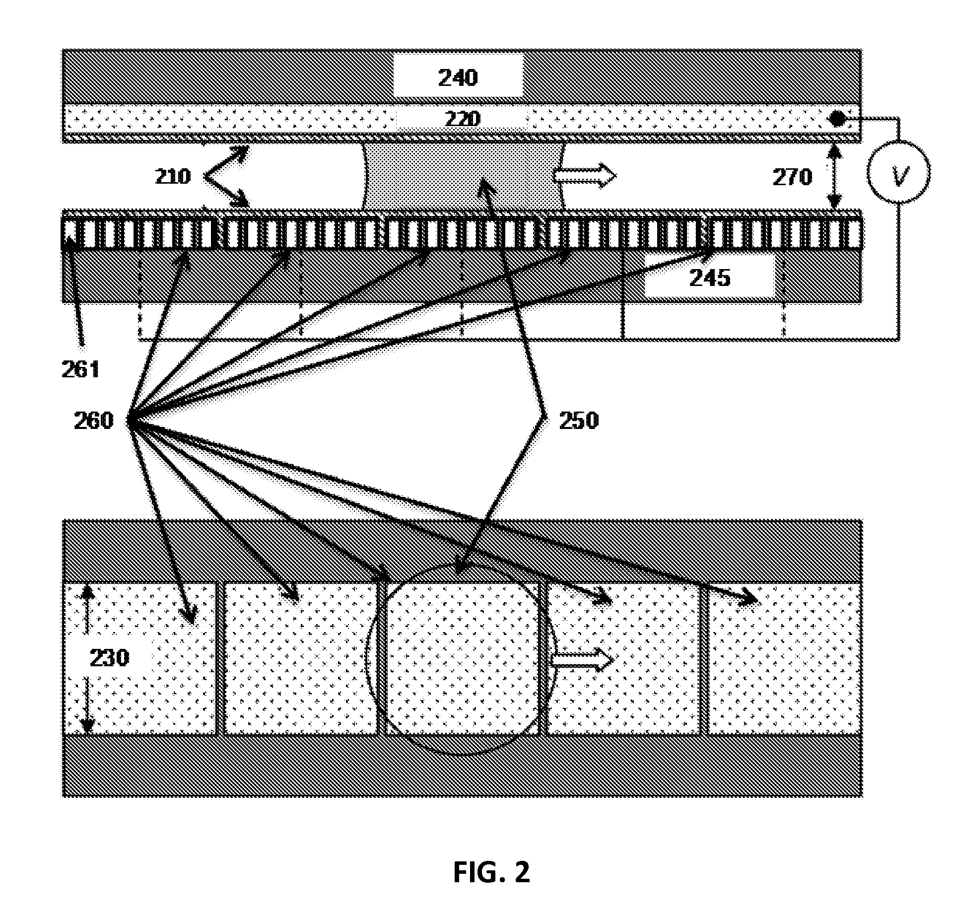
[0097]EWOD based devices are commonly used to manipulate droplets by using the interfacial tension gradient across the gap between the adjacent electrodes to actuate the droplets. The designs of electrodes include the desired shapes, sizes of each of the electrode and the gaps between each of the two electrodes. In the droplet manipulation of EWOD based LOC layout design, the droplet pathways generally are composed of a plurality of electrodes that connect different areas of the design.

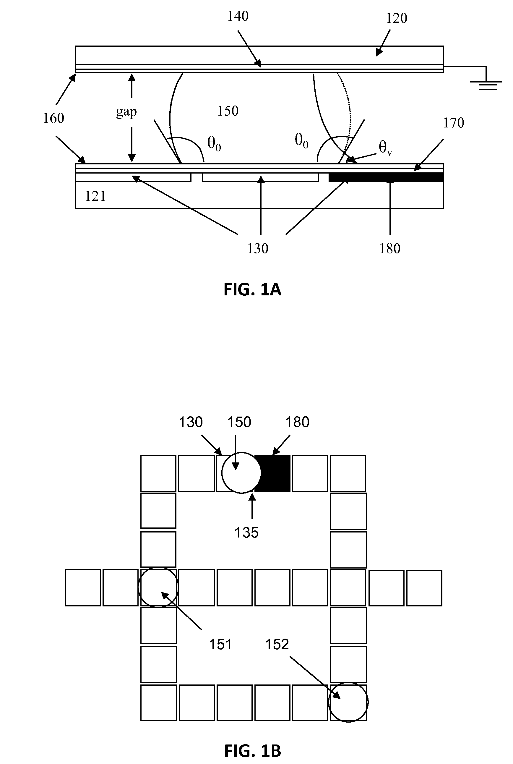
[0098]A conventional electrowetting microactuator mechanism (in small scale for illustration purposes only) is illustrated in FIG. 1A. EWOD-based digital microfluidic device consists of two parallel glass plates 120 and 121, respectively....


PUM

PropertyMeasurementUnit
driving voltageaaaaaaaaaa
velocityaaaaaaaaaa
heightaaaaaaaaaa

Abstract

Disclosed herein is a device A device of the microelectrode array architecture, comprising: (a) a bottom plate comprising an array of multiple microelectrodes disposed on a top surface of a substrate covered by a dielectric layer; wherein each of the microelectrode is coupled to at least one grounding elements of a grounding mechanism, wherein a hydrophobic layer is disposed on the top of the dielectric layer and the grounding elements to make hydrophobic surfaces with the droplets; (b) a field programmability mechanism for programming a group of configured-electrodes to generate microfluidic components and layouts with selected shapes and sizes; and, (c) a system management unit, comprising: (i) a droplet manipulation unit; and (ii) a system control unit.

Description

CROSS REFERENCE TO RELATED APPLICATIONS[0001]The present application claims benefit of priority under 35 U.S.C. 119(e) to: U.S. Patent Application 61 / 312,240, entitled “Field-Programmable Lab-on-a-Chip and Droplet Manipulations Based on EWOD Micro-Electrode Array Architecture” and filed Mar. 9, 2010; U.S. Patent Application 61 / 312,242, entitled “Droplet Manipulations on EWOD-Based Microelectrode Array Architecture” and filed Mar. 9, 2010; U.S. Patent Application 61 / 312,244, entitled “Micro-Electrode Array Architecture” and filed Mar. 10, 2010. The foregoing applications are hereby incorporated by reference into the present application in their entireties.[0002]The present application also incorporates by reference in its entirety co-pending U.S. patent application Ser. No. ______, entitled “Droplet Manipulations on EWOD Microelectrode Array Architecture”, and filed on the same date as the present application, namely, Feb. 17, 2011; co-pending U.S. patent application Ser. No. ______,...

Claims


Application Information

Patent Timeline
Patent Type & Authority Applications(United States)
IPC IPC(8): B81B7/04G06F17/50C25B15/00
CPCB01L3/502792B01L2300/0816B01L2400/0427B01L2300/161B01L2300/089
Inventor WANG, GARY CHORNG-JYHHO, CHING YENHWANG, WEN JANGWANG, WILSON WEN-FU
Owner SPARKLE POWER
Why Eureka
Try Eureka