Semiconductor device having metal gate and manufacturing method thereof

a technology of metal gate and semiconductor, which is applied in the direction of semiconductor devices, electrical devices, transistors, etc., can solve the problems of reducing gate capacitance, inferior performance, and conventional polysilicon gates, so as to avoid high heat budget, improve the filling result of metal layer, and improve reliability

Active Publication Date: 2011-10-13
UNITED MICROELECTRONICS CORP
View PDF2 Cites 59 Cited by
  • Summary
  • Abstract
  • Description
  • Claims
  • Application Information

AI Technical Summary

Benefits of technology

[0009]According to the semiconductor device having metal gate and manufacturing method provided by the present invention, the transistors are fabricated with the gate last process. Since high-temperature processes have already finished before constructing the metal gates of the transistors, the provided method is more applicable to form the transistor needed to avoid high heat budget. Furthermore, the U-type metal layer is provided not only to serve as the required work function metal, but also to improve the filling result of the filling metal layer. Therefore the semiconductor device having metal gate provided by the present invention has the advantage of improved reliability.

Problems solved by technology

However, with a trend toward scaling down the size of the semiconductor device, the conventional polysilicon gate has faced problems such as inferior performance due to boron penetration and unavoidable depletion effect which increases equivalent thickness of the gate dielectric layer, reduces gate capacitance, and worsens a driving force of the devices.
Instead, a roll-off issue is observed.
However, the gate last process still faces integrity requirements for the complicated processes and reliability requirement for the gate trench filling.

Method used


Image

  • Semiconductor device having metal gate and manufacturing method thereof
  • Semiconductor device having metal gate and manufacturing method thereof
  • Semiconductor device having metal gate and manufacturing method thereof

Examples


Embodiment Construction

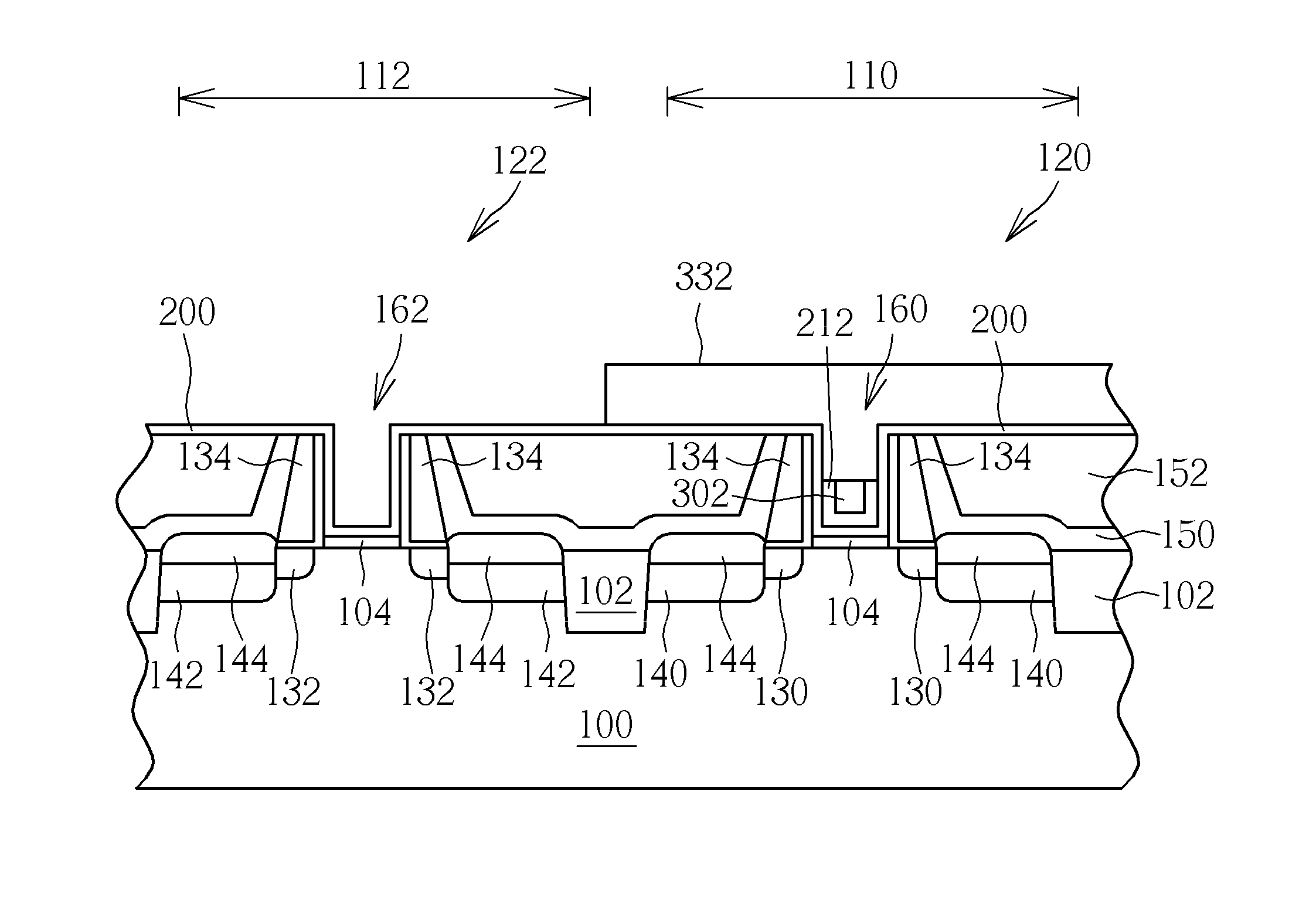
[0013]Please refer to FIGS. 1-8, which are schematic drawings illustrating a method of manufacturing a semiconductor device having metal gate provided by a first preferred embodiment of the present invention. As shown in FIG. 1, a semiconductor substrate 100 is provided. The semiconductor substrate 100 includes silicon substrate, silicon-containing substrate, or silicon-on-insulator (SOI) substrate. A first active region 110 and a second active region 112 are defined on the semiconductor substrate 100 and electrically isolated by a plurality of shallow trench isolations (STIs) 102. Then, a first conductive-type transistor 120 and a second conductive-type transistor 122 are formed on the semiconductor substrate 100 respectively in the first active region 110 and the second active region 112. In the preferred embodiment, the first conductive-type transistor 120 is a p-type transistor and the second conductive-type transistor 122 is an n-type transistor. However, those skilled in the a...


PUM

PropertyMeasurementUnit
work functionaaaaaaaaaa

Abstract

A semiconductor device includes a semiconductor substrate, a gate dielectric layer formed on the semiconductor substrate, and at least a first conductive-type metal gate formed on the gate dielectric layer. The first conductive-type metal gate includes a filling metal layer and a U-type metal layer formed between the filling metal layer and the gate dielectric layer. A topmost portion of the U-type metal layer is lower than the filling metal layer.

Description

BACKGROUND OF THE INVENTION[0001]1. Field of the Invention[0002]The invention relates to a semiconductor device having a metal gate and manufacturing method thereof, and more particularly, to a semiconductor device having a metal gate and manufacturing method applied with a gate last process.[0003]2. Description of the Prior Art[0004]Polysilicon is conventionally used as gate electrode in the semiconductor device, such as the metal-oxide-semiconductor (MOS). However, with a trend toward scaling down the size of the semiconductor device, the conventional polysilicon gate has faced problems such as inferior performance due to boron penetration and unavoidable depletion effect which increases equivalent thickness of the gate dielectric layer, reduces gate capacitance, and worsens a driving force of the devices. Therefore, work function metals are used to replace the conventional polysilicon gate to be the control electrode that competent to the high-K gate dielectric layer.[0005]In a c...

Claims


Application Information

Patent Timeline
Patent Type & Authority Applications(United States)
IPC IPC(8): H01L29/78H01L21/8234
CPCH01L21/823842H01L21/82385H01L29/42372H01L29/7833H01L29/66545H01L29/66583H01L29/6659H01L29/4966
Inventor HWANG, GUANG-YAWYANG, YU-RULIAO, JIUNN-HSIUNGCHOU, PEI-YU
Owner UNITED MICROELECTRONICS CORP
Why Eureka
Try Eureka