Wafer Level Package of MEMS Microphone and Manufacturing Method thereof

Active Publication Date: 2011-10-13
UNITED MICROELECTRONICS CORP
View PDF101 Cites 20 Cited by
  • Summary
  • Abstract
  • Description
  • Claims
  • Application Information

AI Technical Summary

Benefits of technology

[0025]In the wafer level package of MEMS microphone and the manufacturing method of wafer level package of MEMS microphone, the protective layer formed on the supporting rin

Problems solved by technology

Furthermore, a big package stress wil

Method used


Image

  • Wafer Level Package of MEMS Microphone and Manufacturing Method thereof
  • Wafer Level Package of MEMS Microphone and Manufacturing Method thereof
  • Wafer Level Package of MEMS Microphone and Manufacturing Method thereof

Examples


Example

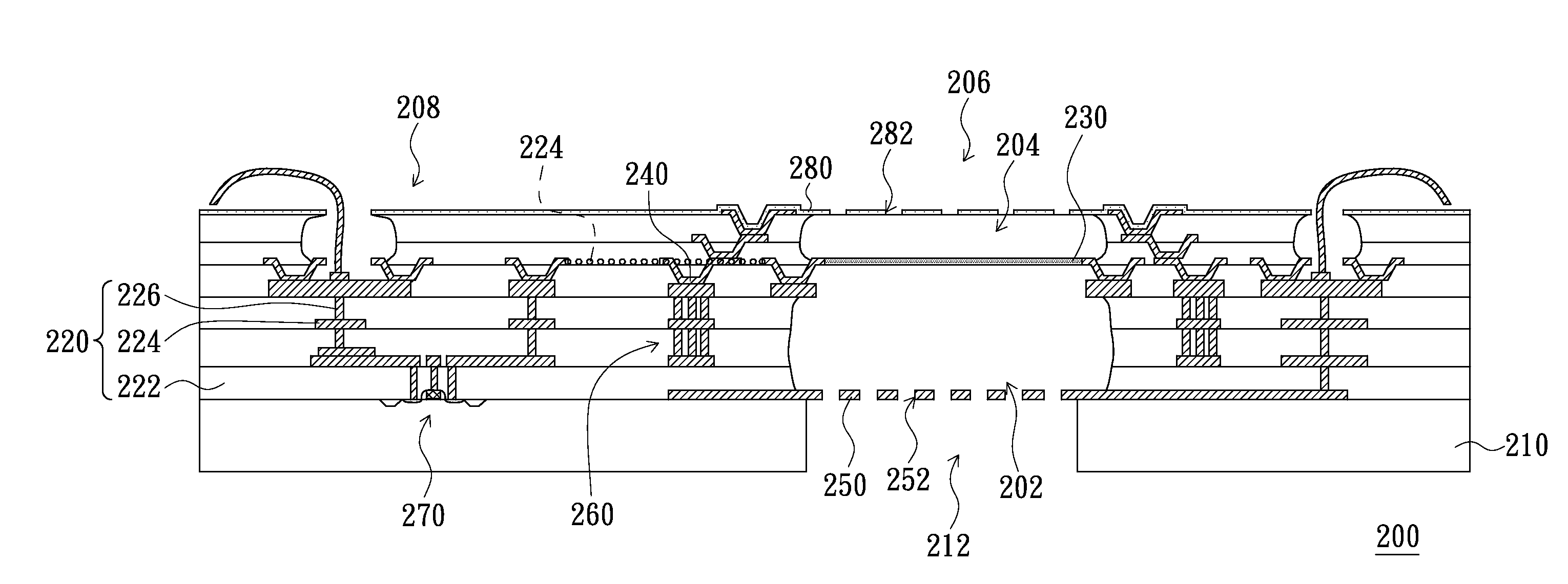
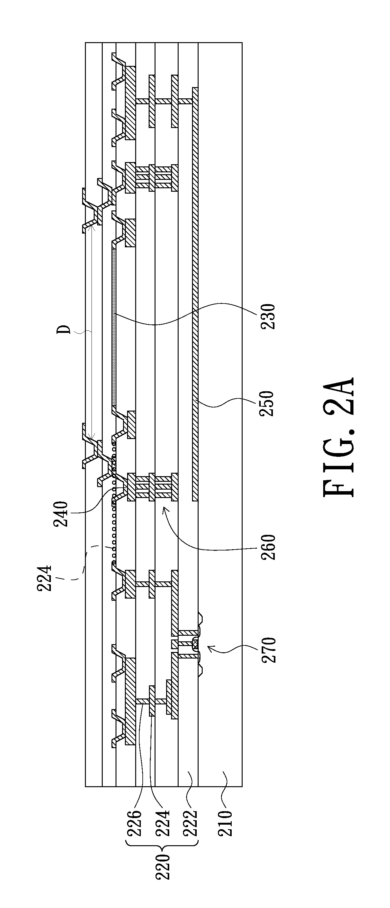
[0029]FIG. 2A to FIG. 2C are schematic flow charts of a manufacturing method for wafer level package of MEMS microphone in accordance with an embodiment of the present invention. Referring to FIG. 2A, in the manufacturing method for wafer level package of MEMS microphone, a number of dielectric layers 222 are formed on a substrate 210 in sequence, a MEMS diaphragm 230 is formed between two adjacent dielectric layers 222 of the dielectric layers 222, and a number of supporting rings 240 are formed in some of the dielectric layers 222 respectively. The supporting rings 240 are stacked with each other. The upmost supporting ring 240 is located in the upmost dielectric layer 222. An inner diameter of the lower supporting ring 240 is greater than that of the upper supporting ring 240. The inner diameter of the supporting ring 240 is labeled by D in FIG. 2A.

[0030]Material of the supporting rings 240 is, for example, metal. In the present embodiment, before the dielectric layers 222 are fo...


PUM

PropertyMeasurementUnit
Dielectric polarization enthalpyaaaaaaaaaa
Electrical conductoraaaaaaaaaa

Abstract

A wafer level package of micro electromechanical system (MEMS) microphone includes a substrate, a number of dielectric layers stacked on the substrate, a MEMS diaphragm, a number of supporting rings and a protective layer. The MEMS diaphragm is disposed between two adjacent dielectric layers. A first chamber is between the MEMS diaphragm and the substrate. The supporting rings are disposed in some dielectric layers and stacked with each other. An inner diameter of the lower supporting ring is greater than that of the upper supporting ring. The protective layer is disposed on the upmost supporting ring and covers the MEMS diaphragm. A second chamber is between the MEMS diaphragm and the protective layer. The protective layer defines a number of first through holes for exposing the MEMS diaphragm. The wafer level package of MEMS microphone has an advantage of low cost.

Description

BACKGROUND[0001]1. Field of the Invention[0002]The present invention relates to a micro electromechanical system (MEMS) microphone, and particularly to a wafer level package of MEMS microphone and a manufacturing method thereof.[0003]2. Description of the Related Art[0004]Micro electromechanical system (MEMS) technique has established a whole new technical field and industry. The MEMS technique has been widely used in a variety of microelectronic devices that have electronic and mechanical properties, for example, pressure sensors, accelerators and micro-microphones. Since the MEMS microphone has the advantages of light, small and high signal quality, it gradually becomes the mainly stream of micro microphone.[0005]FIG. 1 is a schematic view of a conventional package of MEMS microphone. Referring to FIG. 1, the conventional package 100 of MEMS microphone includes a MEMS chip 110 and a complementary metal oxide semiconductor (CMOS) chip 120 disposed on a substrate 130. The MEMS chip ...

Claims


Application Information

Patent Timeline
IPC IPC(8): H01L29/84H01L21/30
CPCB81B7/0061B81B2201/0257B81C2203/0136H04R2201/003H01L2224/48091Y10T29/49005H01L2224/48463H01L2924/1461H01L2924/00014H01L2924/00
Inventor HUANG, CHIEN-HSINCHEN, LI-CHEWANG, MING-ILAN, BANG-CHIANGWU, HUI-MINSU, TZUNG-I
Owner UNITED MICROELECTRONICS CORP
Why Eureka
Try Eureka