

Three-dimensional measuring device and board inspection device
- Summary
- Abstract
- Description
- Claims
- Application Information
AI Technical Summary
Benefits of technology
Problems solved by technology
Method used
Image

Examples
first embodiment
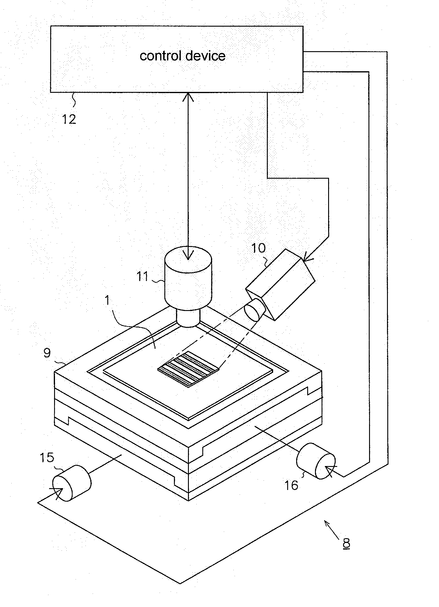
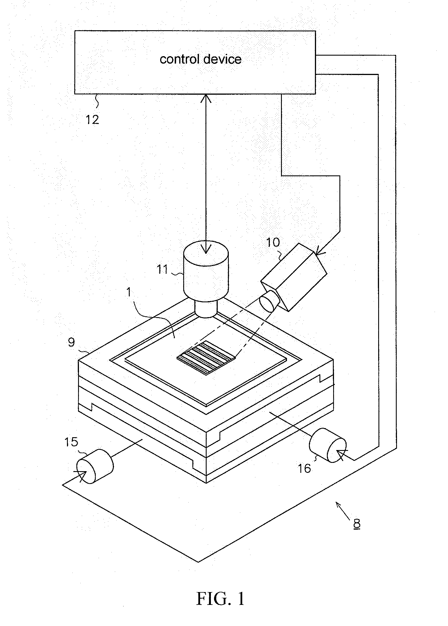
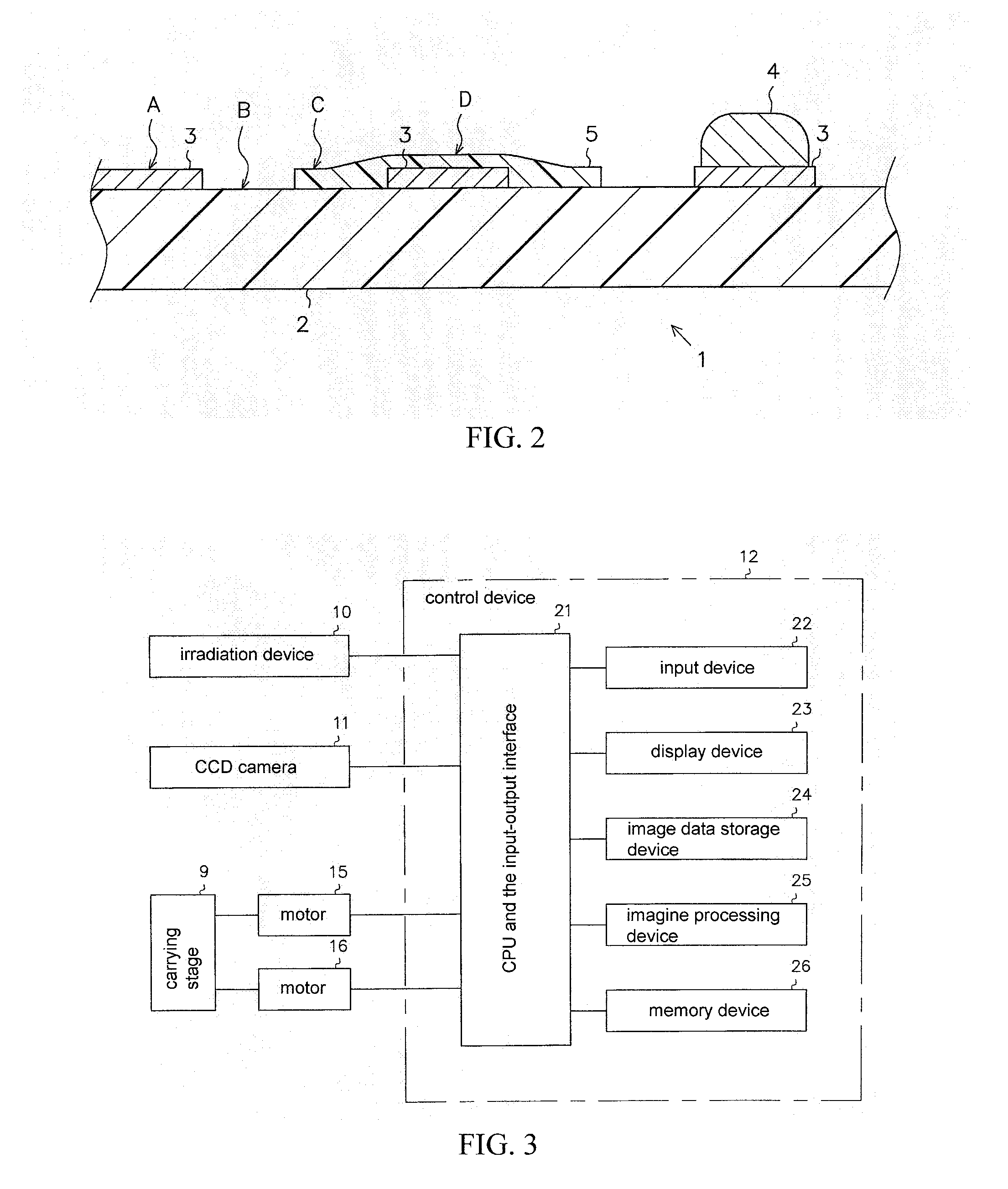
[0043]FIG. 1 is a simplified structural drawing schematically showing the board inspection device equipped with the three-dimensional measuring device of this As shown in this figure, a board inspection device 8 includes a carrying stage 9 for carrying a printed circuit board 1, an irradiation device 10 as an irradiation means for irradiating a certain light component pattern onto the printed circuit board 1 surface from a tilted direction, a CCD camera 11 as an imaging means for imaging of the above-described irradiated part of the printed circuit board 1, and a control device 12 as a control means for execution of various types of control, image processing and calculation processing within the board inspection device 8.
[0044]The above-described carrying stage 9 is equipped with motors 15 and 16. These motors are driven and controlled by the control device 12 so that the printed circuit board 1 carried on the carrying stage 9 can be slid in any x-axis and y-axis direction.
[0045]As...
sixth embodiment
[0076]Alternatively for example, a sixth embodiment is possible in which, when brightness is determined to be saturated among the values obtained by summing the brightness value of each pixel of image data acquired by the first image processing and the brightness value of each pixel of image data acquired by the second image processing means, the brightness value of the image data acquired by the first image processing is used for such a pixel during preparation of image data for three-dimensional measurement, and the above-described summed value is used during preparation of image data for three-dimensional measurement for pixels free of brightness saturation.
[0077]In this manner, even for locations corresponding to bright parts and not just dark parts, use of the above-described summed value is possible when this summed value is free of brightness saturation. Due to dependence of the noise of the CCD, etc. imaging element on the square root of the amount of received light, the dif...
PUM
 Abstract
Description
Claims
Application Information