Process for producing substrate provided with metal pattern and substrate provided with metal laminate
- Summary
- Abstract
- Description
- Claims
- Application Information
AI Technical Summary
Benefits of technology
Problems solved by technology
Method used
Image
Examples
embodiment 1
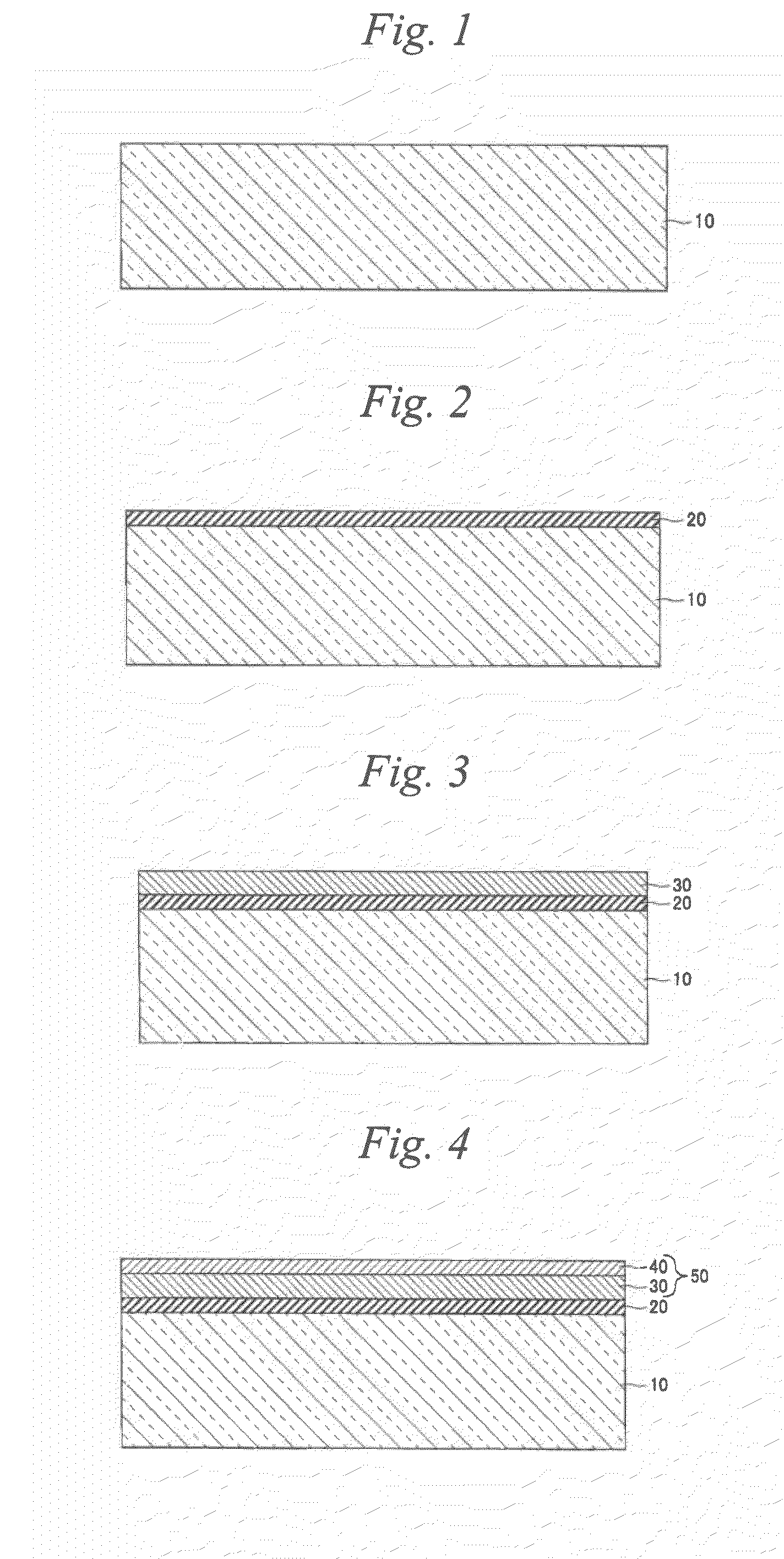
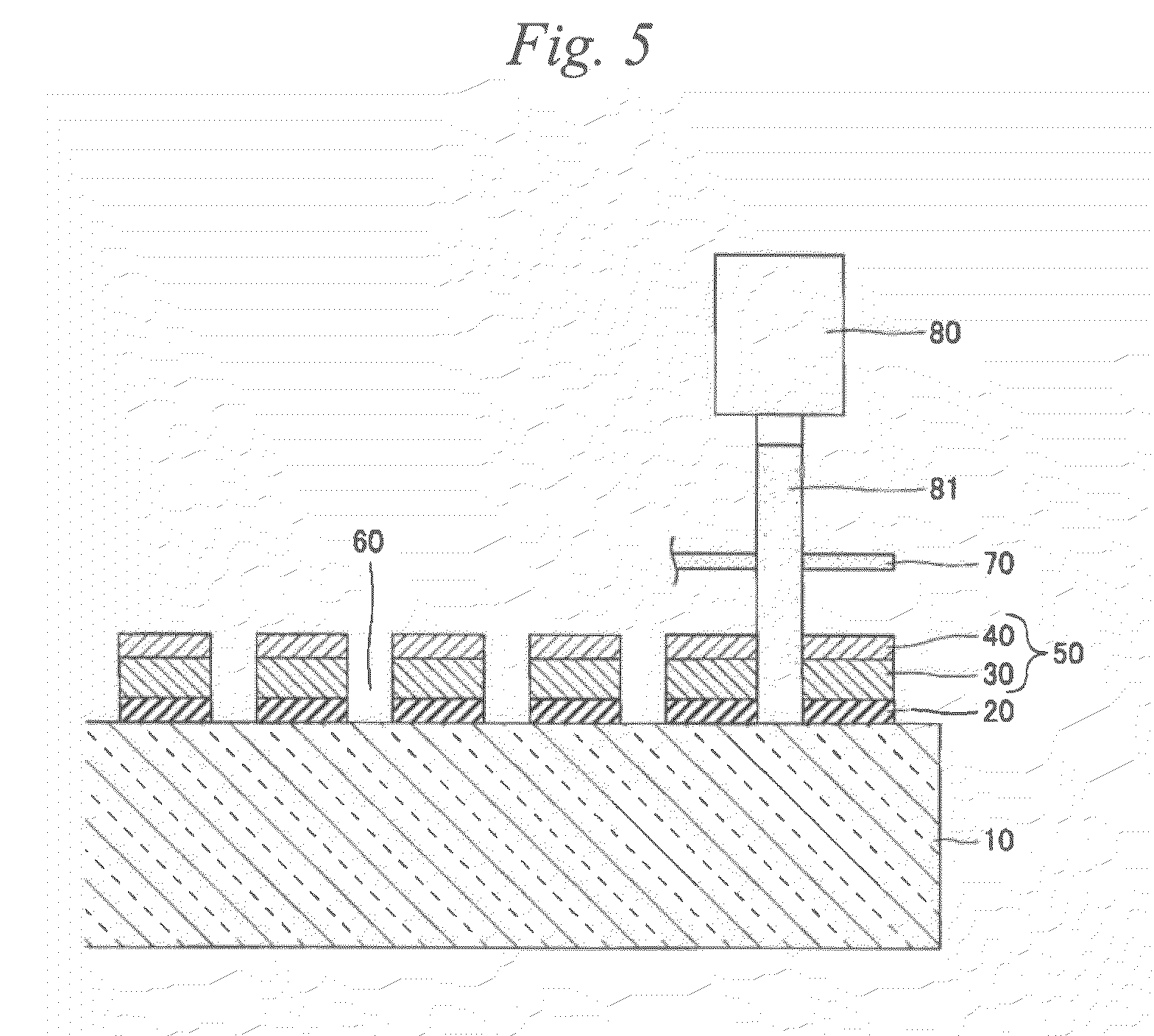
[0065]FIGS. 1 to 7 show one example of respective steps of the process for producing a substrate provided with a metal pattern in accordance with embodiment 1.
[0066]FIG. 1 shows one example of a step of preparing a substrate 10 in the process for producing a substrate provided with a metal pattern in accordance with this embodiment. In FIG. 1, a substrate 10 is shown to be prepared in a mounted state. As the substrate 10, substrates of various materials can be used. For example, a glass substrate 10 is preferably used. The glass substrate 10 is used in many cases as a display panel material of a flat panel display such as a plasma display panel or a liquid crystal panel. In this embodiment, description is made by reference to an example in which a glass substrate is used as the substrate 10. However, various substrates 10 may be used as long as they have resistance to heat to be generated upon laser processing and to laser irradiation thereupon.
[0067]FIG. 2 shows one example of a lo...
embodiment 2
[0106]FIGS. 10 to 14 show one example of the process for producing a substrate provided with a metal pattern in accordance with embodiment 2.
[0107]FIG. 10 shows one example of a step of preparing the substrate 10 in the process for producing the substrate provided with a metal pattern in accordance with embodiment 2. Since the step shown in FIG. 10 is the same as that described with respect to FIG. 1 for embodiment 1, the same reference numbers are given, with descriptions thereon being omitted.
[0108]FIG. 11 shows one example of a metal layer-forming step in the process for producing a substrate provided with a metal pattern in accordance with embodiment 2. In the metal layer-forming step, a metal layer 30 is formed on the substrate 10. In embodiment 1, the low-reflective layer 20 is formed on the substrate 10 whereas, in the process for producing a substrate provided with a metal pattern in accordance with embodiment 2, the low-reflective layer 20 is not formed but the metal layer ...
example 1
[0121]Item (a) in FIG. 15 shows the results of Example 1. In Example 1, a metal layer 30 of copper (Cu) was formed on a substrate 10 for plasma display (PD), and laser processing was conducted. The thickness of the copper metal layer 30 was 2,000 Å. It is seen that, even when a laser light of 74 W in power and 1.2 J / cm2 in fluence was irradiated, the single metal layer 30 composed of Cu was not removed at all though the thickness of the layer was comparatively as thin as 2,000 Å, thus no metal pattern being formed.
PUM
| Property | Measurement | Unit |
|---|---|---|
| Thickness | aaaaa | aaaaa |
| Thickness | aaaaa | aaaaa |
| Length | aaaaa | aaaaa |
Abstract
Description
Claims
Application Information
 - R&D
- Intellectual Property
- Life Sciences
- Materials
- Tech Scout
- Unparalleled Data Quality
- Higher Quality Content
- 60% Fewer Hallucinations
Browse by: Latest US Patents, China's latest patents, Technical Efficacy Thesaurus, Application Domain, Technology Topic, Popular Technical Reports.
© 2025 PatSnap. All rights reserved.Legal|Privacy policy|Modern Slavery Act Transparency Statement|Sitemap|About US| Contact US: help@patsnap.com


