
Method and software for designing semiconductor integrated circuit

a technology of integrated circuits and integrated circuits, applied in the direction of cad circuit design, program control, instruments, etc., can solve the problems of inability to increase the timing failure detection rate at the actual operation frequency, and the difficulty of setting a test, so as to improve the failure detection rate in the layout automatic design process of dft circuits

Inactive Publication Date: 2011-10-27
RENESAS ELECTRONICS CORP
View PDF2 Cites 6 Cited by
  • Summary
  • Abstract
  • Description
  • Claims
  • Application Information

AI Technical Summary

Benefits of technology

[0037]The effects obtained by typical embodiments of the invention disclosed in the present application will be briefly described below.
[0038]The failure detection rate in the layout automatic design process of the DFT circuit can be improved.BRIEF DESCRIPTIONS OF THE DRAWINGS
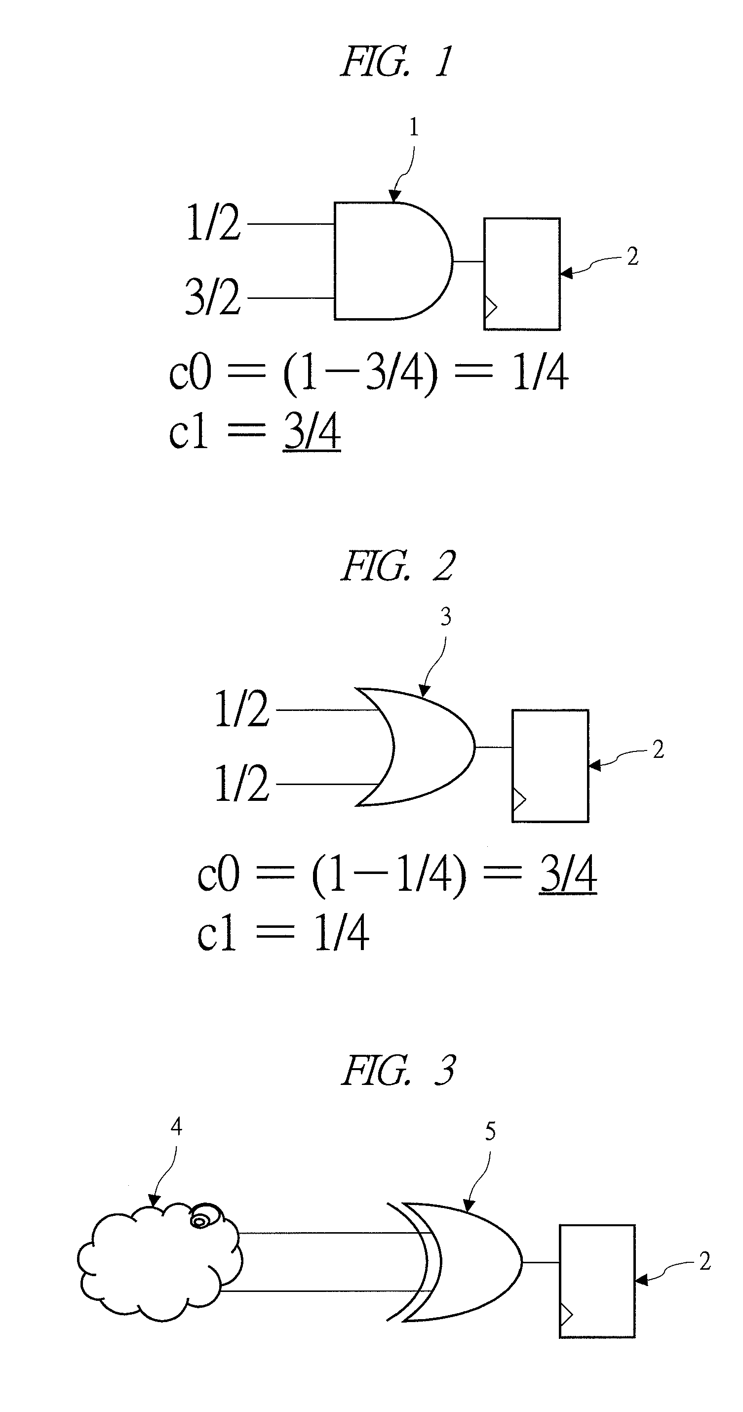
[0039]FIG. 1 is an explanatory diagram showing aggregation conditions of signal lines of a DFT circuit by an AND tree circuit in an layout design process of the DFT circuit according to an embodiment of the present invention;
[0040]FIG. 2 is an explanatory diagram showing aggregation conditions of signal lines of a DFT circuit by an OR tree circuit in an layout design process of the DFT circuit according to an embodiment of the present invention;
[0041]FIG. 3 is an explanatory drawing showing a problem when the signal lines of the DFT circuit are aggregated by an EXOR tree circuit;
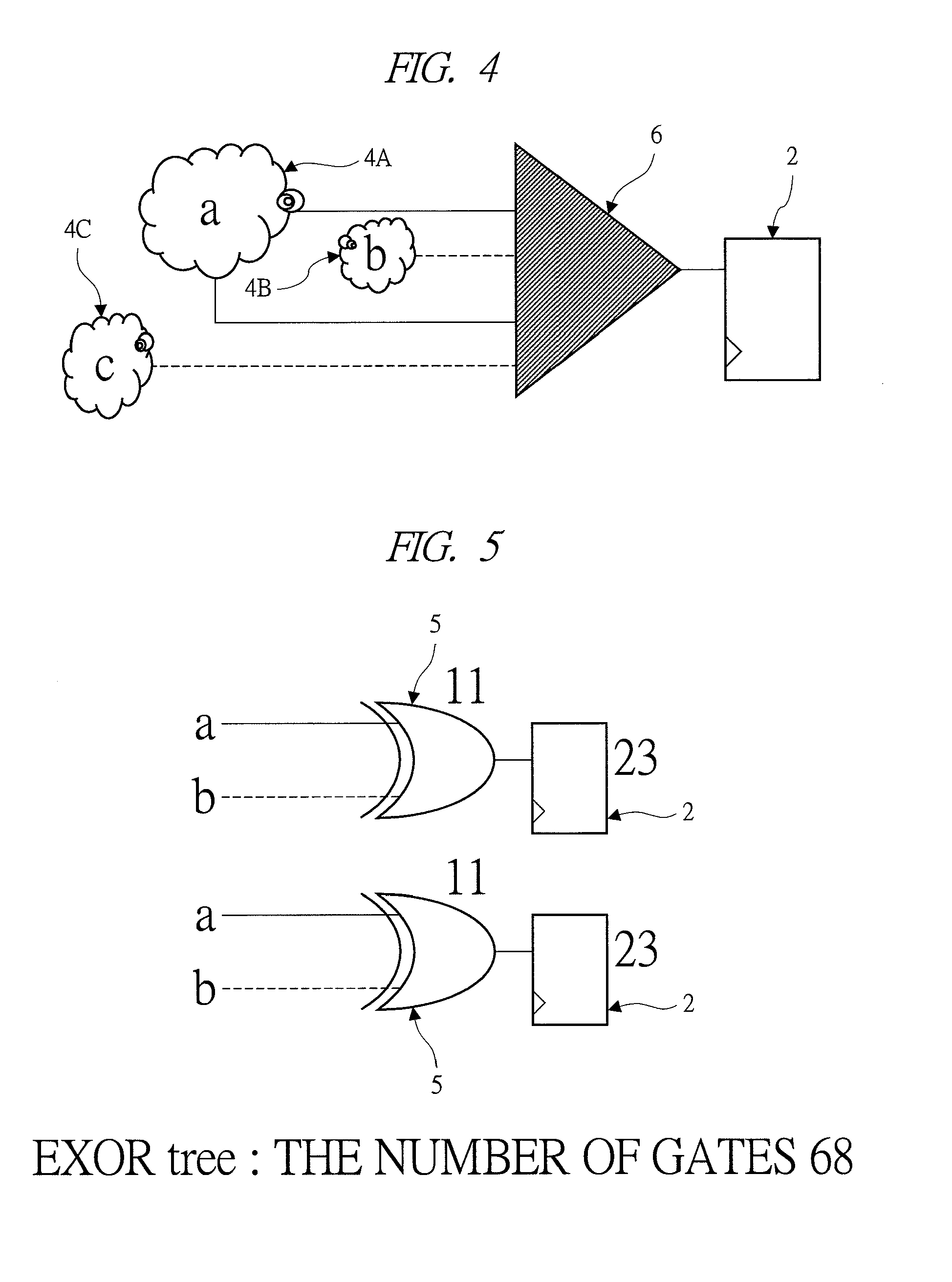
[0042]FIG. 4 is an explanatory drawing showing a tree circuit configuration;

Problems solved by technology

Therefore, it is difficult to set a test pattern that detects a path delay failure, and a timing failure detection rate at the actual operation frequency cannot be increased.

Method used


Image

  • Method and software for designing semiconductor integrated circuit
  • Method and software for designing semiconductor integrated circuit
  • Method and software for designing semiconductor integrated circuit

Examples


Embodiment Construction

[0066]In the embodiments described below, the invention will be described in a plurality of sections or embodiments when required as a matter of convenience. However, these sections or embodiments are not irrelevant to each other unless otherwise stated, and the one relates to the entire or a part of the other as a modification example, details, or a supplementary explanation thereof.

[0067]Also, in the embodiments described below, when referring to the number of elements (including number of pieces, values, amount, range, and the like), the number of the elements is not limited to a specific number unless otherwise stated or except the case where the number is apparently limited to a specific number in principle.

[0068]The number larger or smaller than the specified number is also applicable.

[0069]Further, in the embodiments described below, it goes without saying that the components (including element steps) are not always indispensable unless otherwise stated or except the case whe...


PUM


Abstract

In order to improve a failure detection rate in a layout automatic design process of a DFT circuit, signal lines of the DFT circuit are aggregated by an AND tree circuit 1 or an OR tree circuit instead of an EXOR tree circuit, and outputs thereof are received by an observation flip-flop 2. When a failure detection process of the DFT circuit is performed by using the EXOR tree circuit in the case where partial circuits outputting respective signal lines are shared or the partial circuits have the same structure, the signals cancel each other and the failures of the original partial circuits cannot be detected in some cases. However, such a trouble can be prevented by using the AND tree circuit 1 or the OR tree circuit instead of the EXOR tree circuit.

Description

TECHNICAL FIELD[0001]The present invention relates to a design technology and software of a semiconductor integrated circuit, and more particularly to a technology effectively applied to the layout design process of a DFT (Design For Testability) circuit.BACKGROUND ART[0002]Japanese Unexamined Patent Application Publication No. 2005-223171 (Patent Document 1) discloses a technology for preventing wiring congestion when scan chain groups are connected to constitute a whole scan chain in a semiconductor integrated circuit in which a plurality of scan chain groups are formed. More specifically, when individual scan chain groups are connected to constitute the whole scan chain, the connection sequence of the scan chain groups is determined in order of closeness in mutual distances of the center of gravity coordinates of all the flip-flop layout coordinates included in the respective scan chain groups. Alternately, the connection sequence of the scan chain groups is determined in order o...

Claims


Application Information

Patent Timeline
Patent Type & Authority Applications(United States)
IPC IPC(8): G06F17/50
CPCG06F17/5045G06F30/30
Inventor ISHIKAWA, RYOJI
Owner RENESAS ELECTRONICS CORP
Learn More