

Semiconductor device
a technology of semiconductor devices and inductors, which is applied in the direction of semiconductor devices, semiconductor/solid-state device details, diodes, etc., can solve the problems of insufficient insulation withstand voltage between the two inductors, the inability of the photocoupler to follow an electrical signal, and the inability to reduce the size of the photocoupler, so as to increase the withstand voltage between the first inductor and the second inductor. , the effect of increasing the withstand voltag
- Summary
- Abstract
- Description
- Claims
- Application Information
AI Technical Summary
Benefits of technology
Problems solved by technology
Method used
Image

Examples
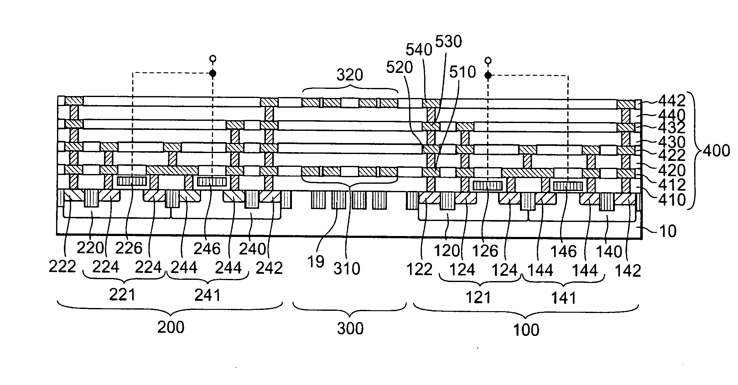
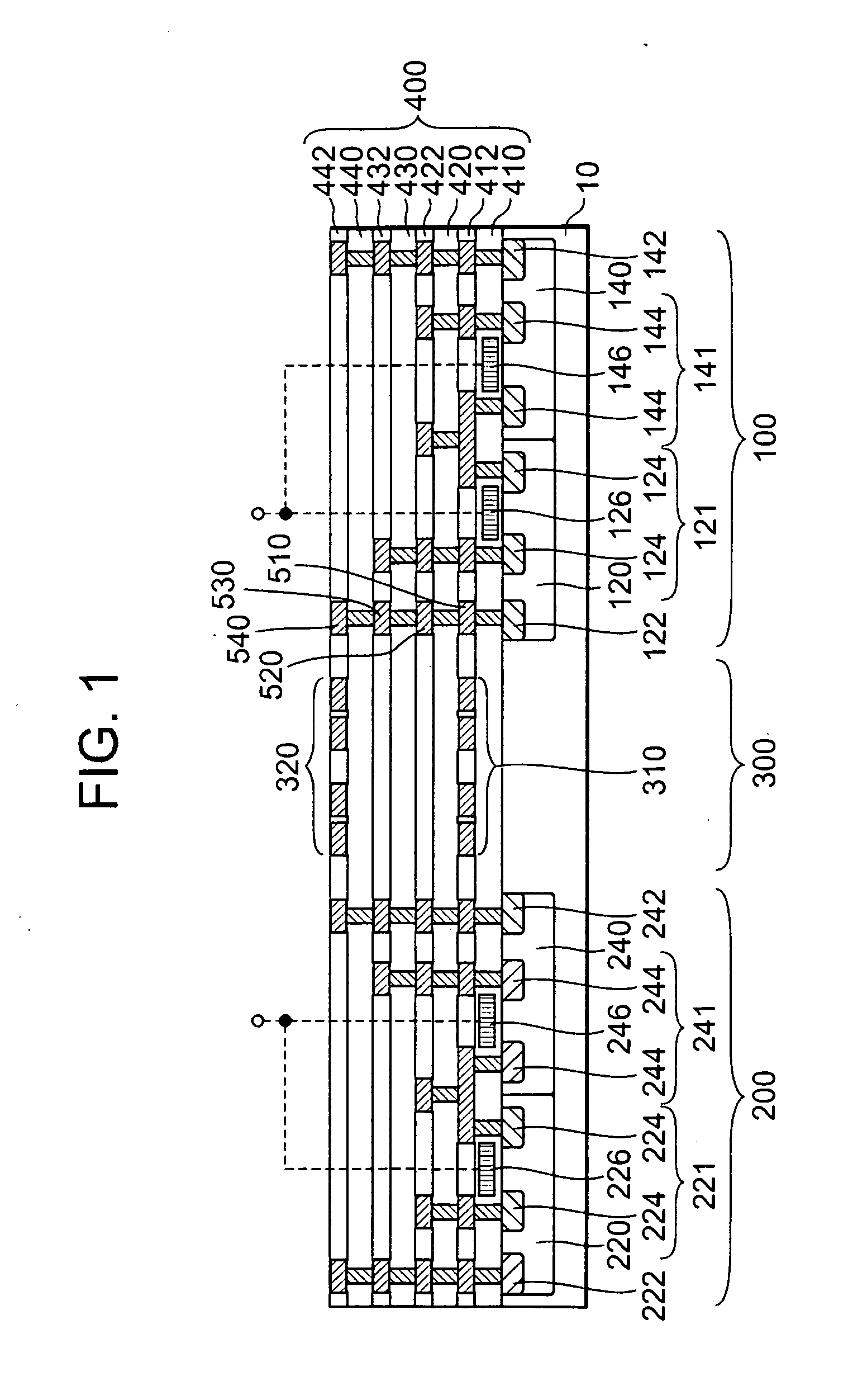
first embodiment
FIG. 1 is a sectional view of a semiconductor device in the This semiconductor device has a substrate 10, a multilayer wiring layer 400, a first inductor 310 and a second inductor 320. The multilayer wiring layer 400, the first inductor 310 and the second inductor 320 are formed on the substrate 10. The multilayer wiring layer 400 is formed by alternately stacking an insulating layer and a wiring layer in this order t or more times (t≧3). The first inductor 310 is provided in the nth wiring layer in the multilayer wiring layer 400. The second inductor 320 is provided in the mth wiring layer in the multilayer wiring layer 400 (t≧m≧n+2) and positioned above the first inductor 310. No inductor is provided in any of the wiring layers positioned between the nth wiring layer and the mth wiring layer to be positioned above the first inductor 310. The first inductor 310 and the second inductor 320 constitute a signal transmitting device 300 which transmits an electrical signal in either of...
fourth embodiment
Also in the present embodiment, the first region and the third region are insulated from the second region in the substrate 10. Therefore the same advantages as those of the fourth embodiment can be obtained. While first region and the third region are electrically connected to each other, the possibility of an increase in potential difference between the first inductor 310 and the substrate 10 is low because the first inductor 310 is connected not to the second circuit 200 but to the first circuit 100. Consequently, the occurrence of dielectric breakdown between the first inductor 310 and the substrate 10 can be reduced even if the first inductor 310 is placed in the lowermost wiring layer 412.
FIG. 7 is a sectional view of a semiconductor device according to the sixth embodiment. This semiconductor device is the same as the semiconductor device according to the fourth embodiment except that a plurality of embedded insulating layers 18 are provided in the substrate 10 below the firs...
sixth embodiment
The same advantages as those of the sixth embodiment can also be obtained by the present embodiment. The same advantages can also be obtained by using an oxide film obtained by local oxidation of silicon (LOCOS) in place of the embedded insulating layer 19.
FIG. 9 is a sectional view of a semiconductor device according to the eighth embodiment. The construction of this semiconductor device is the same as that of the semiconductor device according to the first embodiment except that the embedded insulating layers 19 shown in the seventh embodiment are formed in the substrate 10 below the first inductor 310. In the example shown in FIG. 9, the second inductor 320 can be connected to the second circuit 200 via pads (not shown) formed in the uppermost wiring layer 442 and bonding wires (not shown). With respect to the arrangement shown in FIG. 9, “input electrical signals differ in potential from each other” means that the amplitude (the difference between a potential representing 0 and ...
PUM
 Abstract
Description
Claims
Application Information