Semiconductor device

a technology of semiconductor devices and semiconductors, applied in semiconductor devices, digital storage, instruments, etc., can solve the problems of loss and possible uselessness of remaining regions, and achieve the effect of high integration degr

Inactive Publication Date: 2011-11-10
HITACHI LTD
View PDF3 Cites 22 Cited by
  • Summary
  • Abstract
  • Description
  • Claims
  • Application Information

AI Technical Summary

Benefits of technology

[0015]Referring briefly to the effect obtained by typical inventions among those disclosed in the present application, a phase change memory at high integration degree by using a chalcogenide material can be attained.

Problems solved by technology

When the method of arranging the driving circuits has been studied in details, it has been found that loss may be caused in the layout area in view of the following two points.
Therefore, the remaining region may possibly be a useless region.

Method used


Image

  • Semiconductor device
  • Semiconductor device
  • Semiconductor device

Examples


first embodiment

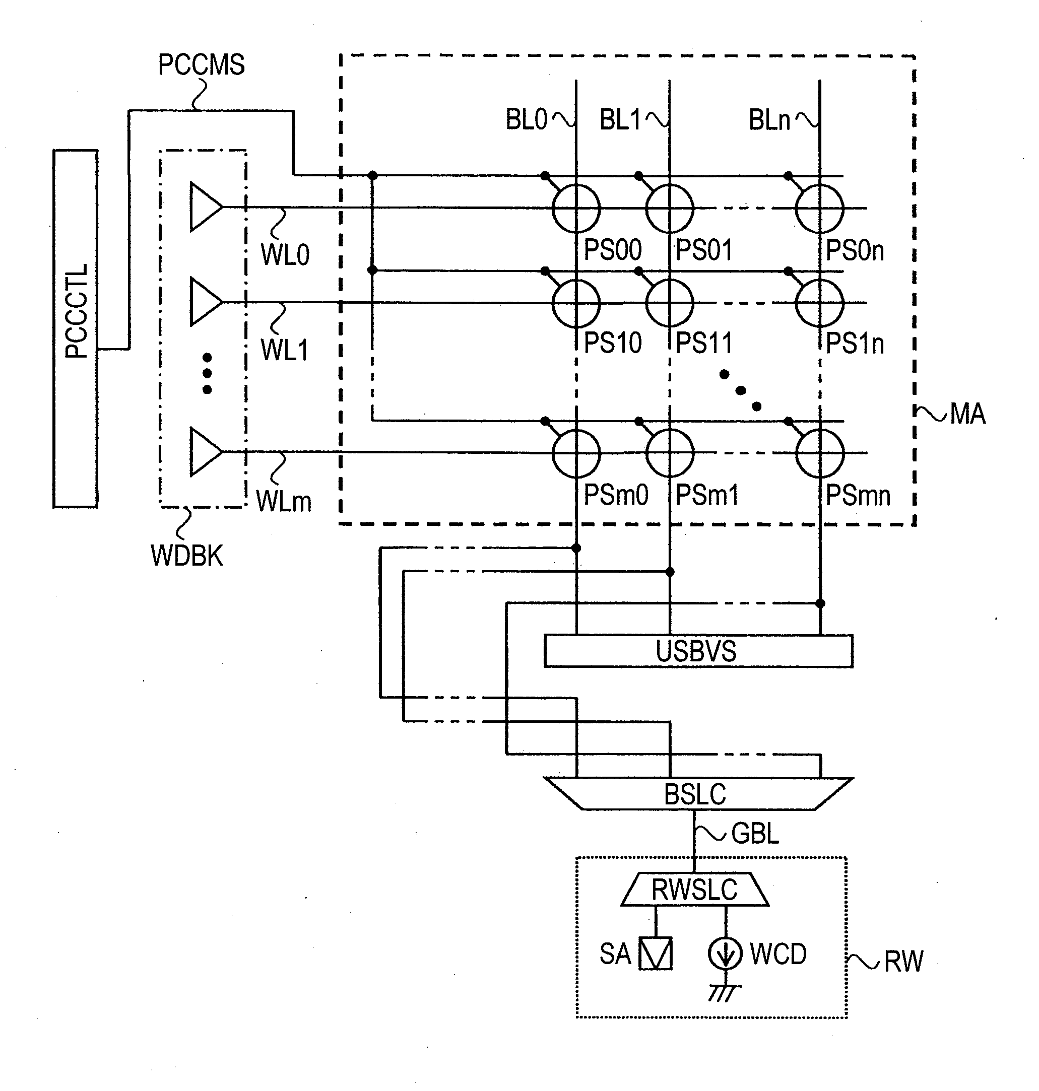
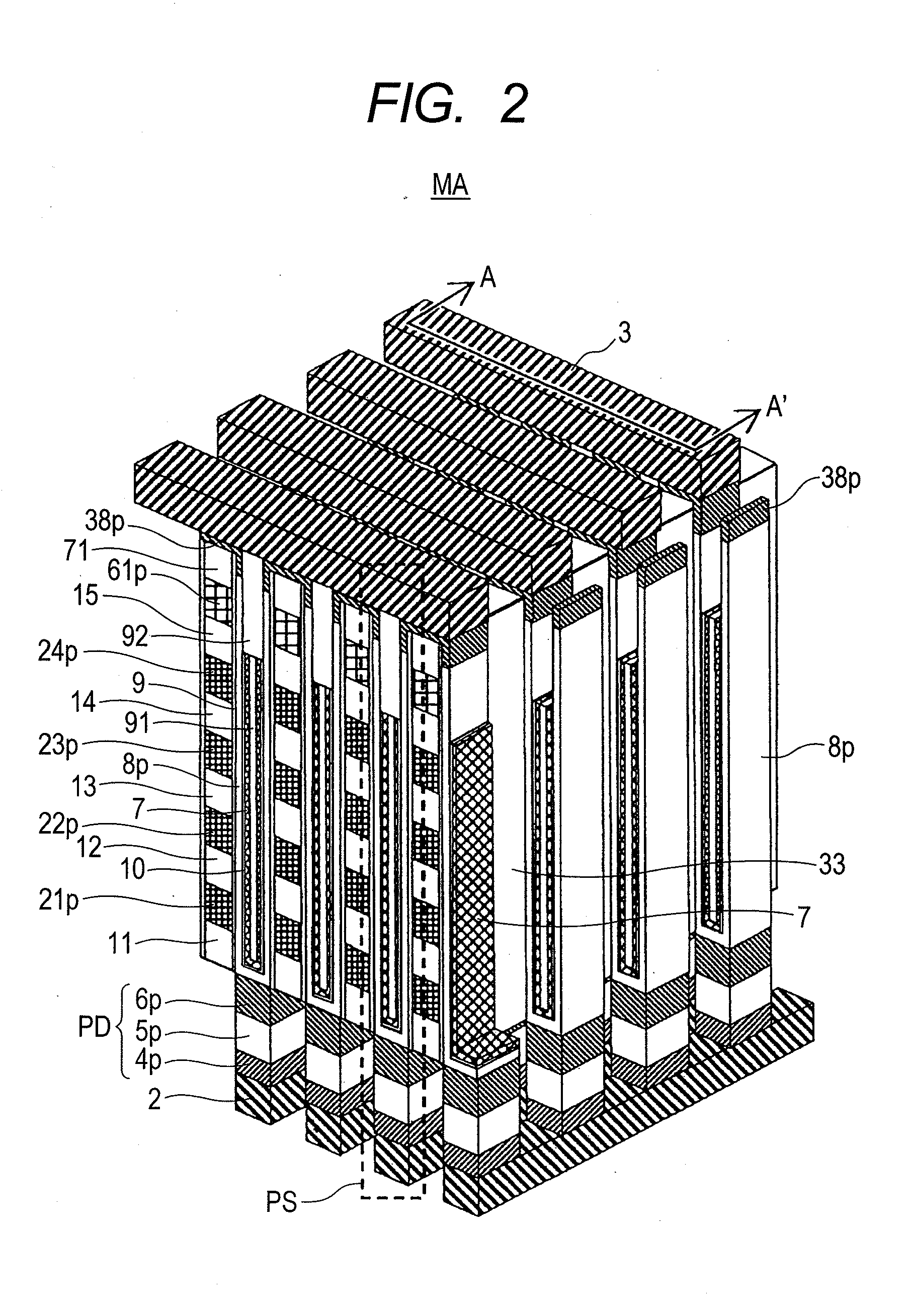
[0038]A preferred embodiment is to be described with reference to an example of a configuration of a memory cell array in which a phase-change-type strings each having a diode and two pairs of phase-change-type chain cells are arranged in a matrix. The phase-change-type chain cell has a configuration in which multiple memory cells are stacked in a direction vertical to a silicon substrate and, further, a transistor for selecting one of phase-change-type chain cells is connected in series further thereover. Further, the memory cell has a configuration in which a select transistor and a phase change device are connected in parallel. Then, the circuit configuration and the structure of the memory cell array are to be described and then the method of arranging various control lines and driving circuits and the operation of the memory cell array are to be described in details.

>

[0039]FIG. 1 shows a memory cell array circuit according to this embodiment. A memory cell array MA includes pha...

second embodiment

[0081]In the first embodiment described above, driving circuits etc. are arranged at the periphery of the memory cell region MAAR as shown in FIG. 8. However, as described above, since the silicon substrate just below the memory cell array region MAAR is an empty place, it is possible to form a portion of the word driver group WDBK, the phase-change-type chain cell control circuit PCCCTL, and the non-select bit line voltage supply circuit USBVS in this region. FIG. 10 is a layout chart schematically showing such an arrangement. In accordance with the layout, the chip area can be decreased. As a result, a low cost phase change memory can be attained.

third embodiment

[0082]In this embodiment, another configuration for the memory cell array of the phase change memory is to be described. This embodiment has the following two features. The first feature is that the memory cell array includes multiple memory tiles. The second feature is that multiple memory tiles use a read / write circuit in common.

[0083]FIG. 11 shows a configuration of a memory cell array according to this embodiment. The drawing shows, as an example, memory tiles MT00 to MT11 each arranged at intersection between the global word line groups GWLMS0 to GWLMS1 and global bit lines GBL0 to GBL1. Each of the memory tiles MT00 to MT11 includes a circuit block excluding the read / write RW from the memory cell array shown in FIG. 1. Read / write circuits RW0 to RW1 are arranged to the global bit lines GBL0 to GBL1, respectively.

[0084]The global word line groups GWLMS0 to GWLMS1 are controlled by a global word driver group GWDBK. Each of the global word line groups GWLMS0 to GWLMS1 has global ...


PUM


Abstract

A semiconductor device has multiple memory cell groups arranged at intersections between multiple word lines and multiple bit lines intersecting the word lines. The memory cell groups each have first and second memory cells connected in series. Each of the first and the second memory cells has a select transistor and a resistive storage device connected in parallel. The gate electrode of the select transistor in the first memory cell is connected with a first gate line, and the gate electrode of the select transistor in the second memory cell is connected to a second gate line. A first circuit block for driving the word lines (word driver group WDBK) is arranged between a second circuit block for driving the first and second gate lines (phase-change-type chain cell control circuit PCCCTL) and multiple memory cell groups (memory cell array MA).

Description

CLAIM OF PRIORITY[0001]The present application claims priority from Japanese patent application JP 2010-107959 filed on May 10, 2010, the content of which is hereby incorporated by reference into this application.FIELD OF THE INVENTION[0002]The present invention concerns a semiconductor device and it relates to a technique which is effective when applied to a storage device including a memory cell including a device causing difference in a resistance value corresponding to stored information and, particularly, it relates to a storage device including a phase change memory using memory cells that store information by utilizing the change of state of a chalcogenide material and discriminating information by detecting the difference of a resistance value depending on the information.BACKGROUND OF THE INVENTION[0003]In the technique investigated by the present inventors, the following techniques may be considered, for example, in a semiconductor device having a phase change memory. The ...

Claims


Application Information

Patent Timeline
Patent Type & Authority Applications(United States)
IPC IPC(8): G11C11/00
CPCG11C13/0004G11C13/0026G11C13/0028G11C13/003H01L45/06H01L45/124G11C2213/78H01L27/2454H01L27/2472H01L27/2481G11C2213/71G11C2213/72G11C2213/75H01L45/144H10B63/34H10B63/84H10N70/231H10N70/8265H10N70/8828H10B63/82
Inventor HANZAWA, SATORUSASAGO, YOSHITSKA
Owner HITACHI LTD
Why Eureka
Try Eureka