

Method of Wafer Level Purifying Light Color Emitting from a Light Emitting Semiconductor Wafer
- Summary
- Abstract
- Description
- Claims
- Application Information
AI Technical Summary
Benefits of technology
Problems solved by technology
Method used
Image

Examples
Embodiment Construction
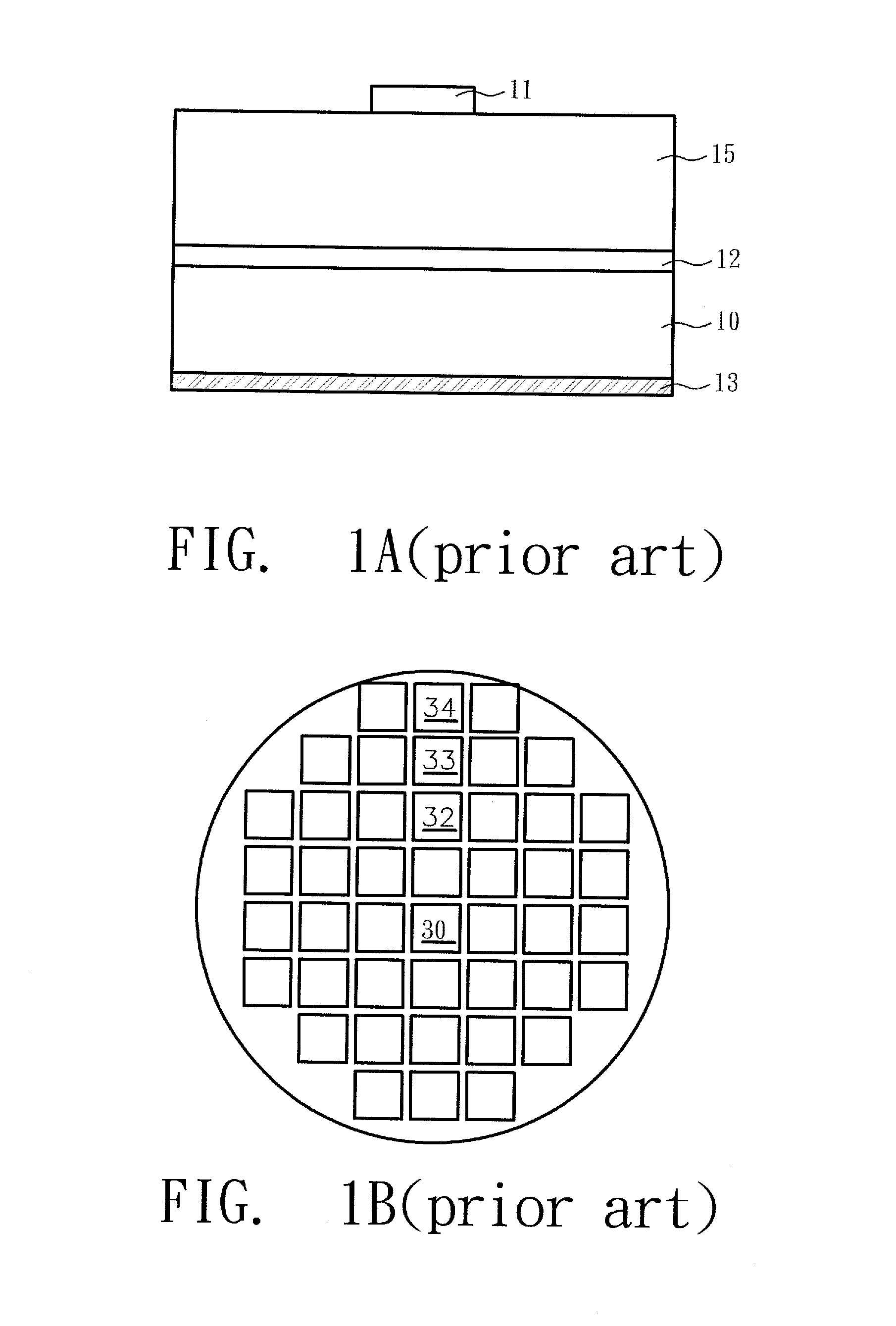
[0015]As aforesaid the conventional LED wafer may have color deviation, e.g. the light emitting from a die located at the center portion of the wafer may be different from that of the die at the edge. While the color deviation out of range, the die may be picked out as an unqualified. Each die of the wafer has to be one-one quality control.
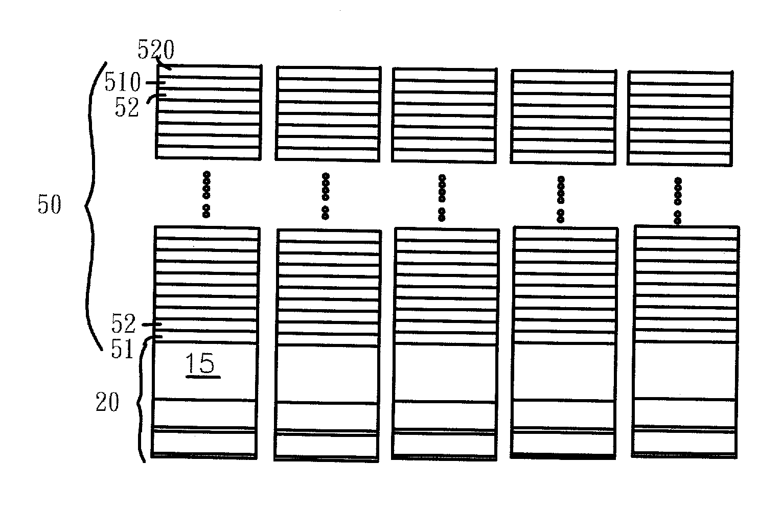
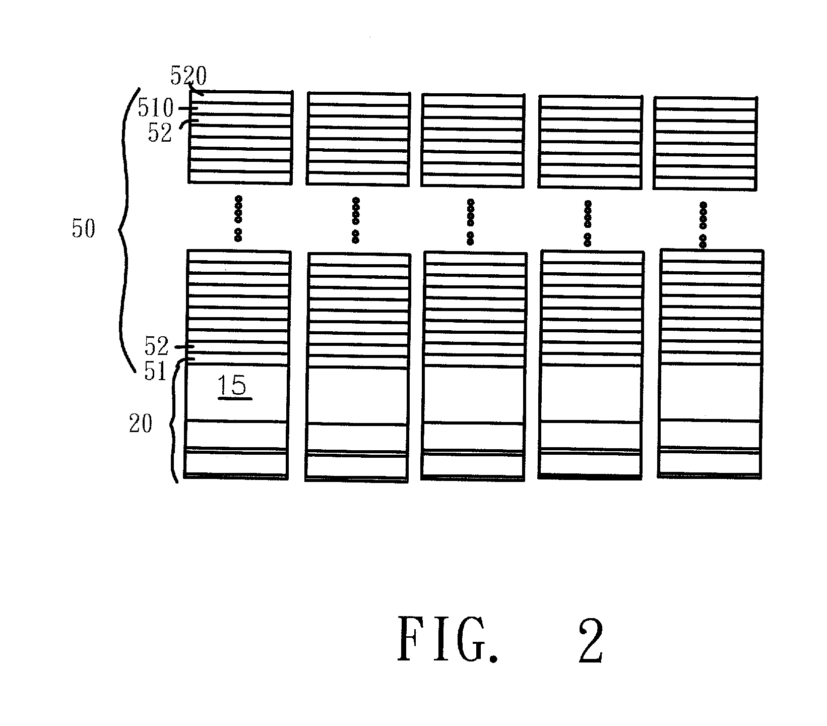
[0016]To overcome the problem, the present invention is to provide a LED wafer formed with multi-transparent layers thereon as a light filter to narrow a wavelength range thereby purifying the color. While the central wavelength of the entire wafer is filtered to a target wavelength, the quality control becomes simple. The QC carried out by picking the dies by just in accordance with illumines, i.e., light intensity. To the downstream LED industries, the quality is more reliable and easy to use.
[0017]The present invention can be applied to any LED wafer including the LED showing FIG. 1A, or the others, and the light may emitting from a single side...
PUM
 Abstract
Description
Claims
Application Information