Single supply sub VDD bitline precharge SRAM and method for level shifting

a single supply, bitline technology, applied in the field of storage arrays, can solve the problems of limiting the scalability of cell transistor dimensions and operating voltage in a conventional cell and static power supply, directly affecting access time and cycle time, and poorly controlling the discharge level of the bitline, so as to improve the sram stability margin and reduce the cell failure rate

Active Publication Date: 2011-11-17
MARVELL ASIA PTE LTD
View PDF3 Cites 23 Cited by
  • Summary
  • Abstract
  • Description
  • Claims
  • Application Information

AI Technical Summary

Benefits of technology

[0007]It is a purpose of the invention to improve SRAM stabil...

Problems solved by technology

However, competing requirements of Read and Write margin improvements on the SRAM cell design limit the scalability of cell transistor dimensions and operating voltages in a conventional cell and static power supplies.
This is because the precharge pulse has to occur before Wordline activation, which directly impacts access time and cycle time.
Furthermore, the discharge level of the Bitline is poorly controlled.
Precharging below the optimum level will cause further degrade in the stability margins.
There are two drawbacks to this design.
One drawback is that the source fol...

Method used


Image

  • Single supply sub VDD bitline precharge SRAM and method for level shifting
  • Single supply sub VDD bitline precharge SRAM and method for level shifting
  • Single supply sub VDD bitline precharge SRAM and method for level shifting

Examples


Embodiment Construction

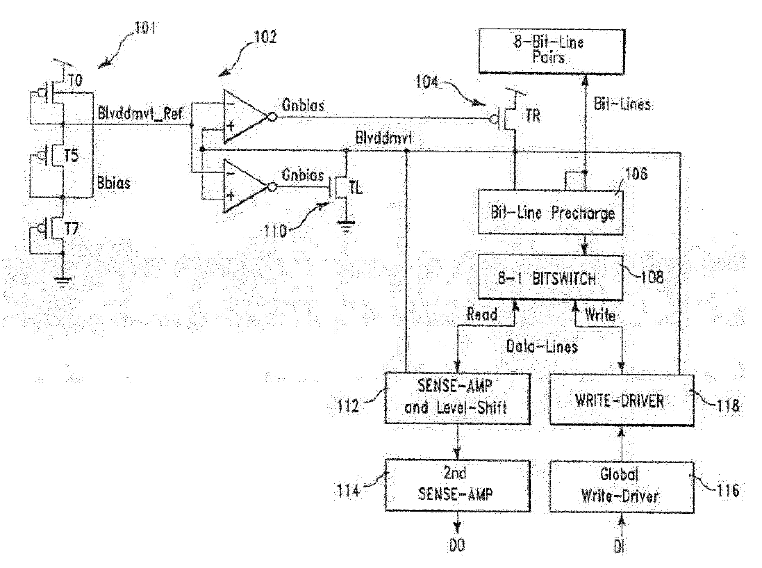
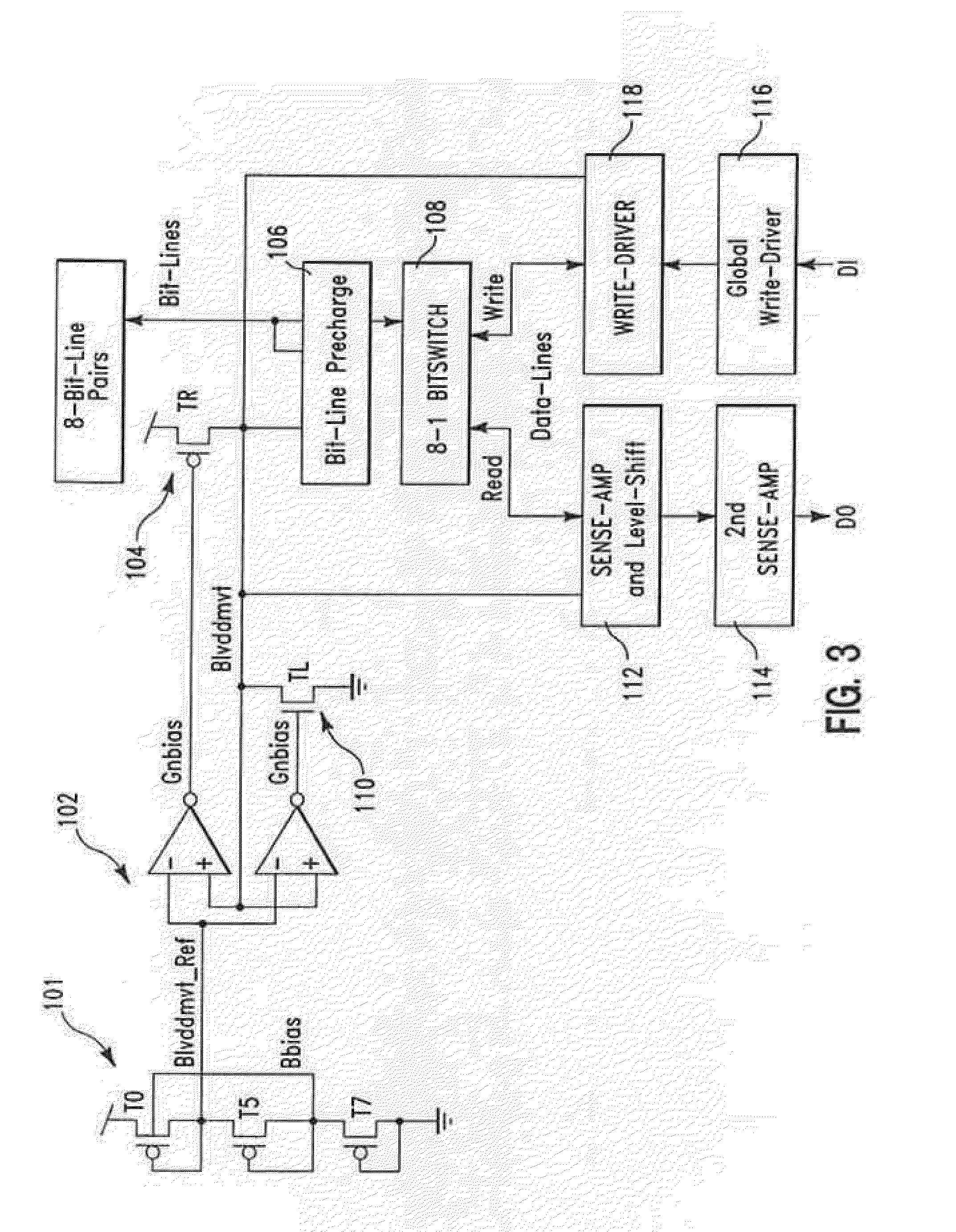
[0021]Turning now to the drawings in greater detail, it will be seen that in FIG. 3 illustrates a block diagram of a preferred embodiment of the present invention that improves SRAM stability. This circuit design provides a bitline precharge with no cycle time pushouts associated with creating a sub-VDD precharge level as well as a self-compensating body-connected bias technique by adjusting the body-contacted bitline precharge device to reduce PVT variations on the pre-charge level. The circuit includes a method for level shifting the sub-VDD sense-amplifier level to a full global data line to the read bit-switch, BL restore, SA restore and write-driver restore which are supplied from Blvddmvt bias power supply (approx. VDD-Vt) to save power and alleviate reliability exposure from the write assist. As shown in FIG. 3 Blvddmvt is generated by a reference source 101 that is connected to a Push-Pull Regulator 102 that is biased with a single, small leakage compensation device 110 and ...


PUM


Abstract

A reduced bitline precharge level has been found to increase the SRAM Beta ratio, thus improving the stability margin. The precharge level is also supplied to Sense amplifier, write driver, and source voltages for control signals. In the sense amplifier, the lower precharge voltage compensates for performance loss in the bit-cell by operating global data-line drivers with increased overdrive. In the write driver, the reduced voltage improves the Bitline discharge rate, improves the efficiency of the negative boost write assist, and decreases the reliability exposure of transistors in the write path from negative boost circuit.

Description

BACKGROUND OF THE INVENTION[0001]1. Field of the Invention[0002]This invention is related to storage arrays, essentially static random access memories (SRAMs) and more particularly to precharging bitlines (BL) to sub-VDD levels.[0003]2. Description of Background[0004]High performance low power SRAM design including multiple local cell groups are well known in the prior art including for example U.S. Pat. Nos. 5,668,761 and 6,657,886. Each cell group includes multiple local cell and local true and complements bitlines. Each SRAM cell includes a pair of inverters that operate together in a loop to store true and complement data. However, competing requirements of Read and Write margin improvements on the SRAM cell design limit the scalability of cell transistor dimensions and operating voltages in a conventional cell and static power supplies. These patents did not employ pre-charging bitlines to sub-VDD levels. During a read operation, SRAM Bitlines are typically precharged to a full...

Claims


Application Information

Patent Timeline
IPC IPC(8): G11C7/00G11C5/14
CPCG11C7/04G11C11/419G11C7/12
Inventor ADAMS, CHAD A.BRACERAS, GEORGE M.NELSON, DANIEL M.PILO, HAROLDRAMADURAI, VINOD
Owner MARVELL ASIA PTE LTD
Why Eureka
Try Eureka