Microfluidic surfaces and devices

a microfluidic surface and microfluidic technology, applied in the field of microfluidic surfaces and devices, can solve the problems of significant behavioral changes, unsuitable for large-scale commercial and industrial applications, and adversely affect the test or process being run

Inactive Publication Date: 2011-11-24
WEB IND
View PDF16 Cites 70 Cited by
  • Summary
  • Abstract
  • Description
  • Claims
  • Application Information

AI Technical Summary

Benefits of technology

[0010]According to a second aspect of the present invention there is provided a method of mass producing microfluidic devices having controlled flow characteristics as a result of the introduction of a non-planar surface topography to the fluid conveying surface of the device, which method comprises (a) creation of a master device whose surface (i) has one or more defined three dimensional images corresponding to one or more defined flow patterns to be imparted to the fluid conveying surface of the microfluidic or lateral flow device or to the stock material from which said microfluidic or lateral flow device element is to be made and (ii) is adapted to impart or transfer to that fluid conveying surface the desired non-planar surface topography and design corresponding to that flow pattern and (b) bringing said master device in contact with said fluid conveying surface so as to impart or transfer the non-planar surface topography to that surface. For example, in one embodiment, the master device may have a negative relief of the desired surface topography whereby when the master device impacts the fluid conveying surface of the microfluidic device or stock material, it imprints the positive relief of the desired non-planar surface topography into the surface thereof. Alternatively, the master device may have incorporated therein or associated therewith capabilities which can establish the desired non-planar topography in the fluid conveying surface through chemical and / or physical transformation means: for example, a chemical etchant, heat, laser ablation, laser etching, differential radiation cure, or some other method or combinations thereof.

Problems solved by technology

However, significant behavioral changes and issues arise in fluid flow on a micro scale: issues related to surface tension, energy dissipation, and fluidic resistance begin to dominate flow characteristics.
For example, a number of these applications require costly equipment making them unsuited for large scale commercial and industrial applications.
Others require the introduction of new chemicals to the system which, if used in specialized analytical processes, can adversely affect the test or process being run.
Some, such as surface treatments and coatings, are only effective over a limited time span.
Still others, like microchannels are less effective or not readily translatable to mass production, at least not in a cost effective manner.

Method used


Image

  • Microfluidic surfaces and devices
  • Microfluidic surfaces and devices
  • Microfluidic surfaces and devices

Examples


example 1

Linear Flow on Nickel Shims

[0057]Sinusoidal wave patterns were produced in the surface of nickel shims using conventional imaging techniques. Specifically, a curable photoresist coating was applied to a glass substrate and subjected to laser imaging using a split laser beam which is manipulated to re-intersect at the coated substrate surface. The laser beams will alternately cancel out each other's energy or amplify each other's energy across the surface of the nickel substrate resulting, in “lines” in the photoresist corresponding to the greater or lesser exposure. The photoresist coated surface is then developed and washed to remove the undeveloped photoresist. The surface is then subjected to electro-plating with nickel to form shims having the negative of the original formed surface topography. A positive shim is likewise prepared by electro-plating of the negative shim. The lines manifest themselves are linear grooves or linear ridges, depending upon whether one, is using the p...

example 2

Linear Flow on Nickel Shims with Cross Grating

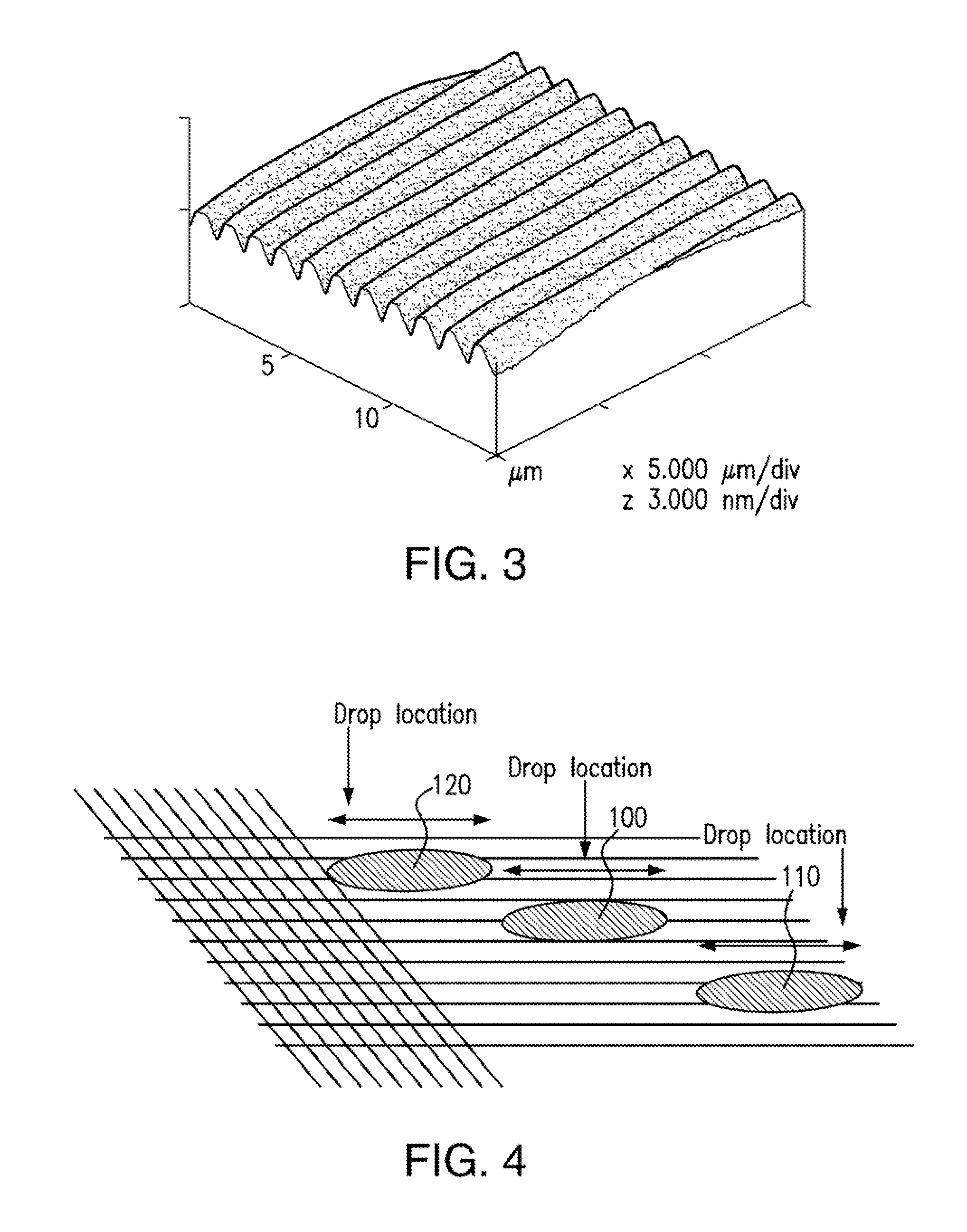
[0060]Nickel shims were prepared as in Example 1 except that a cross-grating was applied. The cross-grating was attained by use of a two-step photoresist curing process wherein the nickel substrate was first exposed as in Example 1 and then the beam to substrate surface angle changed and a the substrate exposed again. This resulted in sample plates that had areas of linear gratings and double gratings superimposed on each other. FIG. 4 presents a schematic of the nickel substrate with the cross-grating topography. Though the pattern is depicted as spaced lines, the actual topography is as shown in FIG. 3; thought the area corresponding to the cross grating would have the same appearance as intersecting waves. The specific samples evaluated and the results attained therewith are presented in Table 2.

[0061]In addition to the quantitative results presented in Table 2, a number of other observations were made and are reflected in the schemat...

example 3

Polymer Substrates

[0062]In order to demonstrate the applicability of the present invention to polymer films, especially with respect to the ability to transfer the surface topography, a number of polymer films were surface modified using the nickel shims from Example 1 as stamping tools. The transfer was effected by an embossing technique in which the heated nickel masters were heat pressed into the polymer film surface using a mechanical press. The heat of the press depended upon the softening point of the specific polymer films selected. Though not used here, the preferential method would be to use a hot rotary embossing process as this is a well known and effective process for embossing polymer films. The surfaces prepared and the results attained thereby are presented in Table 3. In Table 3, the polymer substrates are cyclic olefin copolymer (COC), polycarbonate (PC) and polyethylene terephthalate (PET). Other films being investigated include polyamide, ionomer resin (Surlyn™), ...


PUM

PropertyMeasurementUnit
diameteraaaaaaaaaa
diameteraaaaaaaaaa
heightaaaaaaaaaa

Abstract

Microfluidic surfaces and devices are prepared by imparting a non-planar topography to the liquid flow surface.

Description

RELATED APPLICATION[0001]The present non-provisional patent application claims the benefit of U.S. Provisional Patent Application No. 61 / 347,545 filed on May 24, 2010 and entitled “Microfluidic Surfaces,” the contents of which are hereby incorporated herein in their entirety.[0002]The present application is directed to a method of making microfluidic surfaces as well as microfluidic and lateral flow devices employing said microfluidic surfaces.BACKGROUND OF THE INVENTION[0003]The flow of fluids plays a huge role in society and in industry, how it is effected and controlled, or not controlled, as the case may be, is greatly influenced and affected by the scale of flow of concern. Macrofluidics, or the flow on a macro scale, is most often associated with free surface or channel flow, where, e.g., water follows along the path of least resistance under the influence of gravity, or pressure flow, where fluids are placed under pressure and caused to flow in a desired path. However, in mos...

Claims


Application Information

Patent Timeline
Patent Type & Authority Applications(United States)
IPC IPC(8): F15D1/00B05D5/00B29C59/02B32B3/30
CPCB01L3/502707B01L3/502746B01L2300/0816Y10T428/24479B01L2400/088B29C59/04Y10T428/12389B01L2300/089Y10T137/87249
Inventor GAGNON, JOHN P.
Owner WEB IND
Why Eureka
Try Eureka