Bump structure and fabrication method thereof

a technology of bump structure and fabrication method, which is applied in the direction of printed circuit aspects, sustainable manufacturing/processing, final product manufacturing, etc., can solve the problems of increasing the horizontal width of the bump, the size of the bump in the semiconductor package, and the distance between neighboring bumps becoming extremely narrow, so as to achieve the effect of high soldering post, simplified assembly process, and fine bump structur

Active Publication Date: 2011-11-24
NEPES CO LTD
View PDF2 Cites 22 Cited by
  • Summary
  • Abstract
  • Description
  • Claims
  • Application Information

AI Technical Summary

Benefits of technology

[0015]According to some embodiments of the present invention, a sufficient stand-off height can be secured for a bump structure without increasing solder volume and realizes a fine-pitch bump structure for a semiconductor device. Relatively h

Problems solved by technology

As the integration density of a semiconductor device gets larger and the size of the device gets smaller, bumps in semiconductor package becomes smaller and the distance between neighboring bumps becomes extremely narrow.
Solder bump is transformed during reflow process into spherical shape, which causes the increase of

Method used


Image

  • Bump structure and fabrication method thereof
  • Bump structure and fabrication method thereof
  • Bump structure and fabrication method thereof

Examples


Embodiment Construction

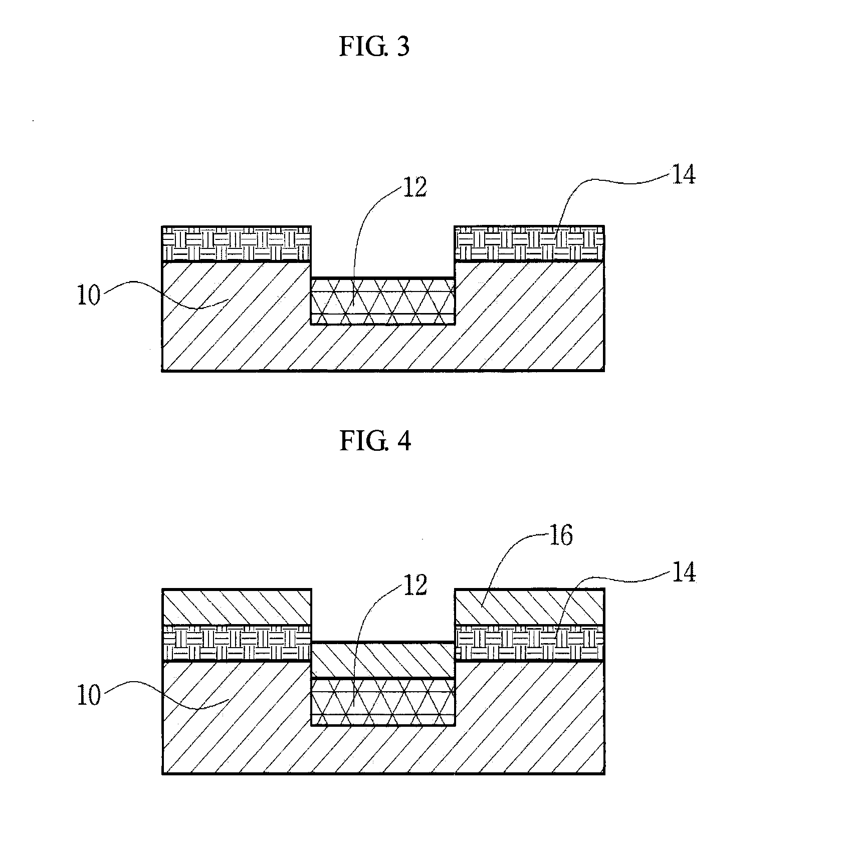
[0026]The present invention will now be described more fully hereinafter with reference to the accompanying drawings, in which preferred embodiments of the invention are shown.

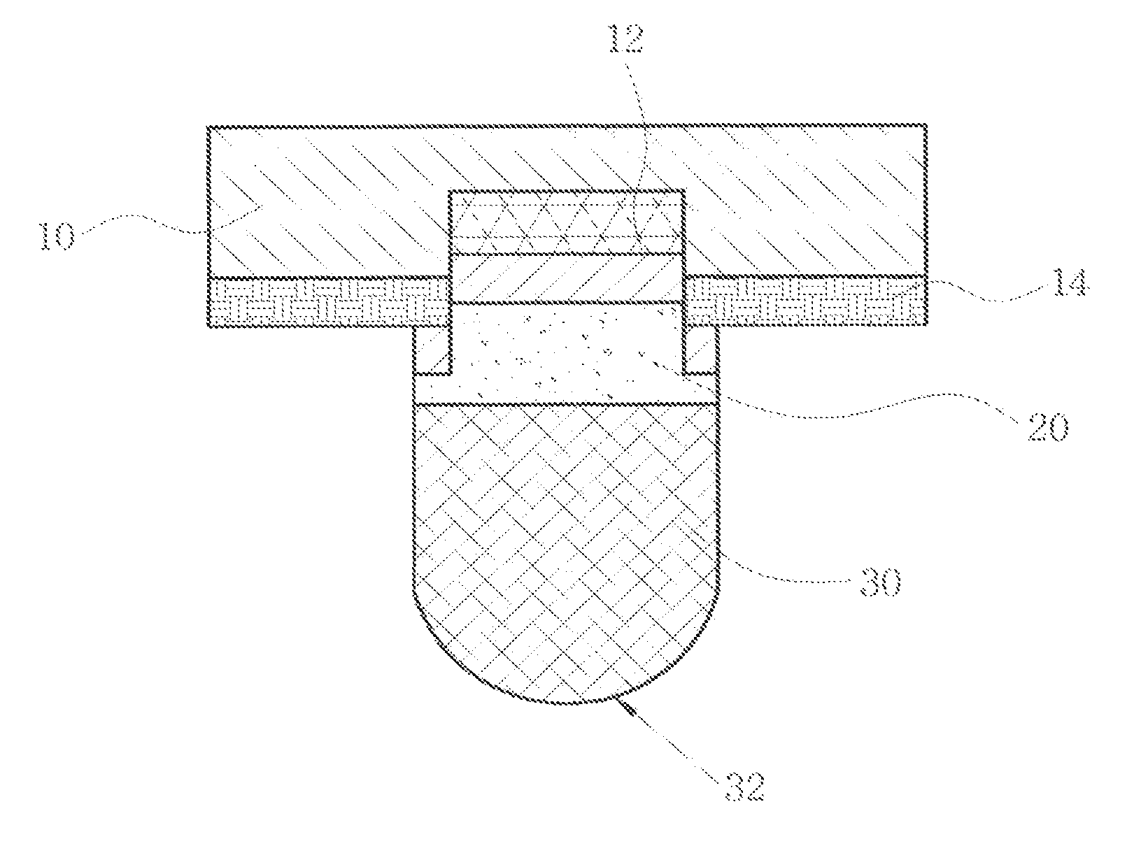
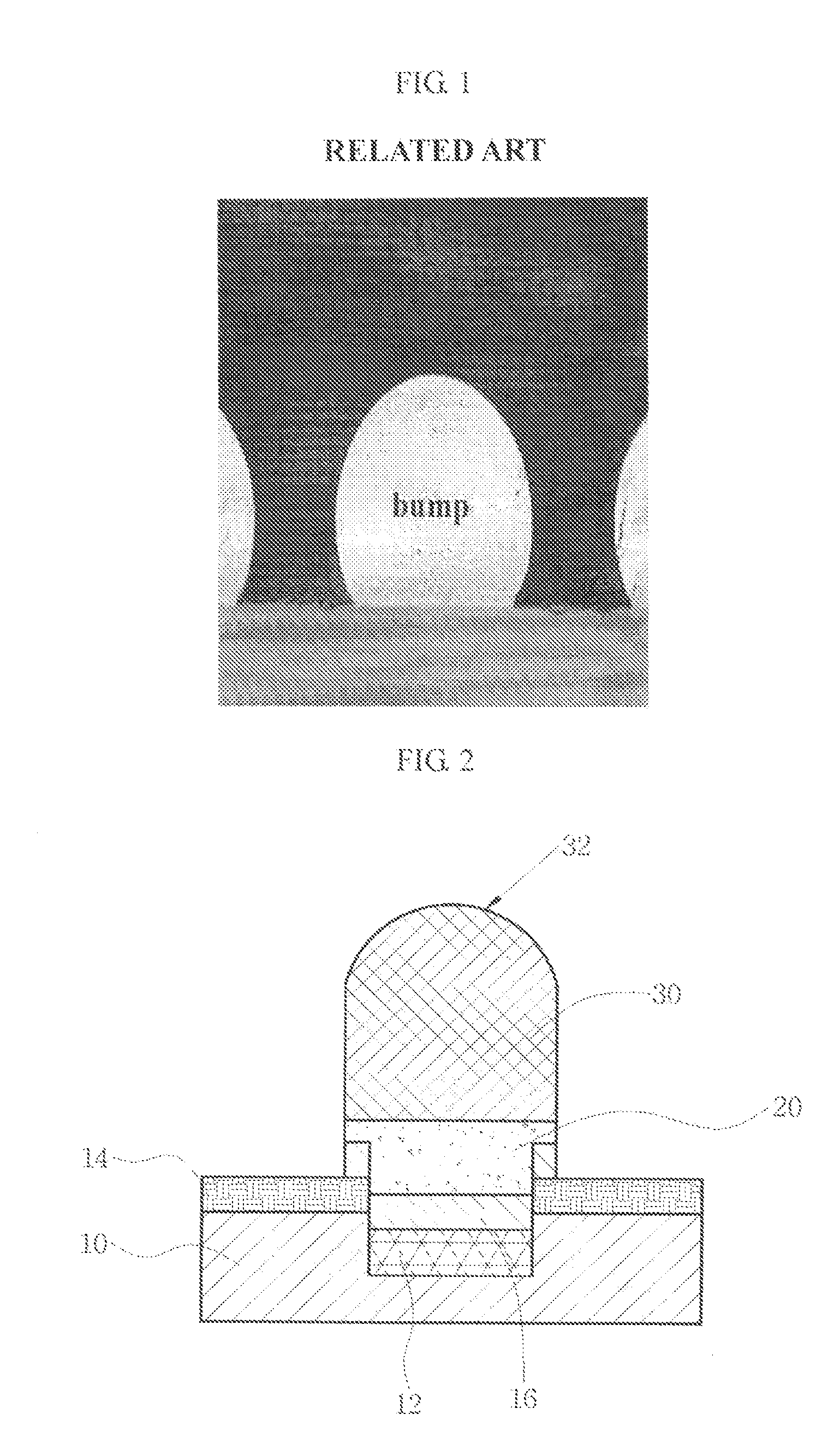
[0027]The present invention provides a pillar type bump structure with a metal post and a solder post, and the main feature of the present invention is that an oxide layer formed on the bump structure prevents the solder post from transforming into a spherical shape in a reflow step.

[0028]FIG. 2 shows a sectional view of a bump structure in accordance with the present invention. The bump structure includes a metal post (20) in the lower part and a solder post (30) in the upper part. The metal post (20) and the solder post (30) form a single body with a cylindrical shape, and have the same horizontal width. The height of the bump structure is larger than the width. That is, the bump structure has high aspect ratio. This leads to sufficient stand-off height (SOH) for the bump structure, resulting in easy surface...


PUM


Abstract

There is provided a bump structure for a semiconductor device, comprising a metal post formed on and electrically connected to an electrode pad on a substrate, a solder post formed on the top surface of the metal post, said solder post having the same horizontal width as the metal post and the top surface of the solder post being substantially rounded, and an intermetallic compound layer disposed at the interface between the metal post and the solder post. An oxide layer formed on the solder post prevents solder post under reflow from being changed into a spherical shape. An intermetallic compound layer may be formed by an aging process at the interface between the metal post and the solder post. The bump structure can realize fine pitch semiconductor package without a short between neighboring bumps.

Description

CROSS-REFERENCE TO RELATED APPLICATIONS[0001]This application claims priority and the benefit of Korean Patent Application No. 10-2010-47802 filed on May 23, 2010 in the Korean Intellectual Property Office, the entire contents of which are incorporated herein by reference.BACKGROUND[0002]1. Technical Field[0003]The present disclosure relates to a bump structure for a semiconductor device, and more particularly, to a new bump structure and a fabrication method thereof for fine pitch semiconductor package.[0004]2. Discussion of Related Art[0005]As personal computers, portable phones, personal information terminals and electronic products have become small, light and been functionalized, data processing capacity has greatly increased. In accordance with this tendency, a wafer level chip scale package to be very close to the size of a semiconductor chip is regarded in semiconductor packages.[0006]Generally, in the wafer level chip scale package, a wafer is packaged and cut after a wafer...

Claims


Application Information

Patent Timeline
IPC IPC(8): H01L23/498H01L21/3205
CPCH01L23/13H01L23/49811H01L24/03H01L24/05H01L24/11H01L24/13H01L24/16H01L24/81H01L24/93H01L2224/03462H01L2224/03464H01L2224/0348H01L2224/03912H01L2224/0401H01L2224/056H01L2224/11462H01L2224/1181H01L2224/1182H01L2224/11848H01L2224/11849H01L2224/119H01L2224/13016H01L2224/13017H01L2224/13082H01L2224/13083H01L2224/131H01L2224/13111H01L2224/13144H01L2224/13147H01L2224/13155H01L2224/16237H01L2224/81385H01L2224/814H01L2224/81815H01L2224/93H01L2924/01013H01L2924/01025H01L2924/01029H01L2924/01079H01L2924/014H05K3/3436H05K3/3478H05K2201/09472H01L2924/01006H01L2924/01023H01L2924/01024H01L2924/01033H01L2924/0105H01L2924/01074H01L2924/01327H01L2924/00014H01L2224/11H01L2924/14H01L2224/1148H01L2224/11474H01L2224/0347H01L2224/10126H01L2224/02126H01L2224/11901Y02P70/50H01L2924/00
Inventor SONG, CHI JUNGKANG, IN SOOJUNG, GI JOPARK, YUN MOOKLEE, EUNG JULEE, JUN KYULEE
Owner NEPES CO LTD
Why Eureka
Try Eureka